Showing posts with label driver. Show all posts
Showing posts with label driver. Show all posts
Saturday, September 20, 2014
Electric Guitar Preamp Mixer and Line Driver
Depending on its design an electric guitar may have anything from one to six pickup elements. Classic (acoustic) guitars could also benefit from one or more retro-fitted pickups. Each pickup has a specific sound depending on the type of sensor and the location on the instrument. When a guitar has more than one pickup these can be connected together with or without additional components. However it is preferable for each pickup signal to be buffered individually. These buffered and possibly amplified signals should be level-adjusted in order to produce the desirable effect (or ‘sound’). After that they are mixed and sent to the next stage of the audio processing equipment.
Circuit diagram:
Most guitarists agree that pickup elements cannot drive cables longer than about 6 feet without risking significant signal degradation. Guitar pickups typically require a load resistance above 50 kΩ and sometimes higher than 200 kΩ, hence a preamplifier/buffer is often inserted, whose main function is not high gain but to enable cables between 10 and 30 feet to be connected representing a capacitance between 90 and 180 pF/m. In the circuit shown here, each pickup has its own input buffer with a transistor configured as an emitter follower. Each stage has a gain slightly lower than unity. This is not an issue because most pickups provide significant signal levels, typically well over 200 mVpp.
The input resistance of the first stage exceeds 200 kΩ, which is appropriate for most inductive pickups on the market. If higher input resistance is needed the 1-MΩ resistors marked with asterisks could be omitted, and the 720-kΩ ones may be increased to 1.2 – 1.5 MΩ. This will raise the stage’s input resistance to around 500 kΩ. To ensure the highest possible undistorted signal can be developed at the output of the first stages, the collector-emitter voltage (VCE) of T1–T4 should be about half the supply voltage. It is important for the first transistor in the buffer to have low noise and high DC gain.
The types BC549C and BC550C and the venerable BC109C are perfectly suitable in this respect while the BC546C, BC547C and BC548C may also be considered. The buffered signal from each pickup is adjusted with a potentiometer and sent to the summing circuit of the mixer. The next active element is an audio operational amplifier type NE5534 or NE5534A (IC1), which provides the required amount of signal buffering. The 5534(A) has low noise, low distortion and high gain. It can drive a 600 Ω line when necessary, but the preferred load is above 2 kΩ. Its amplification is adjustable between 3 and 10 with feedback potentiometer P5. At higher values of the gain some limiting and distortion of the output signal is ‘achieved’, which may well be a desirable side effect.
The maximum undistorted amplitude of the output signal depends on the supply voltage. If higher gain is needed the value of P5 may be increased to 470 kΩ. Output K7 has a volume control potentiometer (P6), which could be omitted if not used or required. Both outputs K6 and K7 are capable of driving 600 Ω loads including high-impedance headphones. The circuit is simple to test and adjust, as follows:
Continue reading...
Circuit diagram:

Electric Guitar Preamp, Mixer and Line Driver Circuit Diagram
Most guitarists agree that pickup elements cannot drive cables longer than about 6 feet without risking significant signal degradation. Guitar pickups typically require a load resistance above 50 kΩ and sometimes higher than 200 kΩ, hence a preamplifier/buffer is often inserted, whose main function is not high gain but to enable cables between 10 and 30 feet to be connected representing a capacitance between 90 and 180 pF/m. In the circuit shown here, each pickup has its own input buffer with a transistor configured as an emitter follower. Each stage has a gain slightly lower than unity. This is not an issue because most pickups provide significant signal levels, typically well over 200 mVpp.
The input resistance of the first stage exceeds 200 kΩ, which is appropriate for most inductive pickups on the market. If higher input resistance is needed the 1-MΩ resistors marked with asterisks could be omitted, and the 720-kΩ ones may be increased to 1.2 – 1.5 MΩ. This will raise the stage’s input resistance to around 500 kΩ. To ensure the highest possible undistorted signal can be developed at the output of the first stages, the collector-emitter voltage (VCE) of T1–T4 should be about half the supply voltage. It is important for the first transistor in the buffer to have low noise and high DC gain.
The types BC549C and BC550C and the venerable BC109C are perfectly suitable in this respect while the BC546C, BC547C and BC548C may also be considered. The buffered signal from each pickup is adjusted with a potentiometer and sent to the summing circuit of the mixer. The next active element is an audio operational amplifier type NE5534 or NE5534A (IC1), which provides the required amount of signal buffering. The 5534(A) has low noise, low distortion and high gain. It can drive a 600 Ω line when necessary, but the preferred load is above 2 kΩ. Its amplification is adjustable between 3 and 10 with feedback potentiometer P5. At higher values of the gain some limiting and distortion of the output signal is ‘achieved’, which may well be a desirable side effect.
The maximum undistorted amplitude of the output signal depends on the supply voltage. If higher gain is needed the value of P5 may be increased to 470 kΩ. Output K7 has a volume control potentiometer (P6), which could be omitted if not used or required. Both outputs K6 and K7 are capable of driving 600 Ω loads including high-impedance headphones. The circuit is simple to test and adjust, as follows:
- check that VCE on T1–T4 is approximately half the supply voltage;
- with no input signal, adjust trimpot P7 for about half the supply voltage at the output of IC1. If precise regulation of the opamp’s output offset is not required P7 may be omitted and R17 connected to the junction of R18 and R19.
Author: Petre Tzvetanov Petrov (Bulgaria) - Copyright: Elektor Electronics 2011

Thursday, September 5, 2013
Bidirectional Motor Control Using L293 Driver
Using the L293 quadruple high-current half-H driver integrated circuit can be designed a very simple high efficiency motor control. The L293 is designed to provide bidirectional drive currents of up to 1 A at voltages from 4.5 V to 36 V. The L293D is designed to provide bidirectional drive currents of up to 600-mA at voltages from 4.5 V to 36 V.
Bidirectional Motor Control Circuit Diagram

Each output is a complete totem-pole drive circuit, with a Darlington transistor sink and a pseudo-Darlington source. Drivers are enabled in pairs, with drivers 1 and 2 enabled by 1,2EN and drivers 3 and 4 enabled by 3,4EN. When an enable input is high, the associated drivers are enabled and their outputs are active and in phase with their inputs. When the enable input is low, those drivers are disabled and their outputs are off and in the high-impedance state. With the proper data inputs, each pair of drivers forms a full-H (or bridge) reversible drive suitable for solenoid or motor applications.
External high-speed output clamp diodes should be used for inductive transient suppression. In this bidirectional stepper motor controller electronic project VCC1 is logic supply and must me between 4.5 and 7 volts ( typically 5 volt) and VCC2 is the power supply for the motor and must be from VCC1 up to 36 volts.
Bidirectional Motor Control Circuit Diagram

Each output is a complete totem-pole drive circuit, with a Darlington transistor sink and a pseudo-Darlington source. Drivers are enabled in pairs, with drivers 1 and 2 enabled by 1,2EN and drivers 3 and 4 enabled by 3,4EN. When an enable input is high, the associated drivers are enabled and their outputs are active and in phase with their inputs. When the enable input is low, those drivers are disabled and their outputs are off and in the high-impedance state. With the proper data inputs, each pair of drivers forms a full-H (or bridge) reversible drive suitable for solenoid or motor applications.
External high-speed output clamp diodes should be used for inductive transient suppression. In this bidirectional stepper motor controller electronic project VCC1 is logic supply and must me between 4.5 and 7 volts ( typically 5 volt) and VCC2 is the power supply for the motor and must be from VCC1 up to 36 volts.
Wednesday, September 4, 2013
Dimming Controlled LED Driver Using LM3409
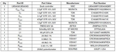
This dimming controlled LED driver circuit is designed using LM3409 P-channel MosFET controller for step-down (buck) current regulators.The LM3409 devices use Constant Off-Time (COFT) control to regulate an accurate constant current without the need for external control loop compensation Dimming controlled LED driver electronic circuit require an input voltage of 36 volts and will provide at output a voltage of 24 volts at a maximum current of 700mA.
Dimming Controlled LED Driver Circuit Diagram

Parts List:
Dimming Controlled LED Driver Circuit Diagram
Parts List:

LED Driver for Automotive Applications using AT9933
Using the AT9933 variable frequency PWM controller IC, can be designed a very simple and high efficiency LED lamp driver using a low-noise boost-buck topology.The AT9933 uses patent pending hysteretic current-mode control to regulate both the input and the output currents.
This enables superior input surge immunity without the necessity for complex loop compensation. Input current control enables current limiting during startup, input under-voltage and output overload conditions. The AT9933 provides a low-frequency PWM dimming input that can accept an external control signal with a duty cycle of 0 - 100% and a high dimming ratio.
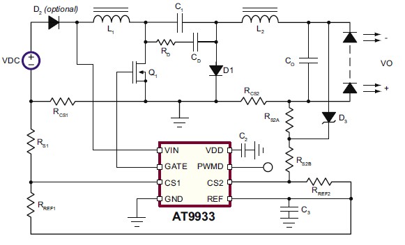
This LED driver electronic project , require an input voltage range between 9 and 16 volts and will provide an 28 volt output at a maximum output current of 350 mA .The switching frequency of this electronic project is 350kHz . Values for components are : L1 = 82μH,L2 = 150μH,C1 = 0.22μF , RCS2 = 1.65Ω 1/4W, RREF2 = 10kΩ 1/8W, RS2A = 100Ω 1/8W,RS2B = 5.23kΩ 1/8W, RCS1 = 0.228Ω 1W, RREF1 = 10kΩ 1/8W,RS1 = 4.42kΩ 1/8W .
This enables superior input surge immunity without the necessity for complex loop compensation. Input current control enables current limiting during startup, input under-voltage and output overload conditions. The AT9933 provides a low-frequency PWM dimming input that can accept an external control signal with a duty cycle of 0 - 100% and a high dimming ratio.
This LED driver electronic project , require an input voltage range between 9 and 16 volts and will provide an 28 volt output at a maximum output current of 350 mA .The switching frequency of this electronic project is 350kHz . Values for components are : L1 = 82μH,L2 = 150μH,C1 = 0.22μF , RCS2 = 1.65Ω 1/4W, RREF2 = 10kΩ 1/8W, RS2A = 100Ω 1/8W,RS2B = 5.23kΩ 1/8W, RCS1 = 0.228Ω 1W, RREF1 = 10kΩ 1/8W,RS1 = 4.42kΩ 1/8W .
Monday, September 2, 2013
Gu10 LED Light Bulbs Driver Schematic
A very simple high efficiency Gu10 led light bulbs driver power supply circuit that can be used as a LED driver for GU10 lamp can be designed using this schematic circuit.This high efficiency Gu10 led light bulbs LED driver is designed to drive 12 V at 0.3 A from an input voltage range of 90 VAC to 265 VAC using few external components.
This Gu10 led light bulbs driver power supply uses the LNK605DG IC from the LinkSwitch-II family by Power Integrations. The LNK605DG provides a sophisticated range of protection features including auto restart for open control loop and output short-circuit conditions. As you can see in the circuit diagram , this LED driver require few external electronic components .The LNK605DG Ic from LinkSwitch-II family is an integrated controller plus 700 V power MOSFET intended for use in LED driver or charger applications.
Gu10 LED Light Bulbs Driver Circuit Diagram

The rectified and filtered input voltage is applied to one end of the primary inding of T1 transformer and the other side of the transformer’s primary winding is driven by the integrated 700 V power MOSFET in U1. The leakage inductance drain voltage spike is limited by an RCDR clamp consisting of D1, R3, R4, and C3.
The secondary of the transformer is rectified by D3 ( a Schottky barrier type was selected for higher efficiency) and filtered by C7. Resistor R1 and C6 dampen high frequency ringing and reduce the diode voltage stress The T1 transformer must have 30 turns from NC to pin1( with 0.221 mm copper wire) , 80 turns from pin1 to pin 2 ( with 0.15 mm copper wire) , 15 turns from pin7 to pin8 ( with 0.4mm copper wire) and 16 turns from pin A to pin B (using 0.2mm copper wire ) .
This Gu10 led light bulbs driver power supply uses the LNK605DG IC from the LinkSwitch-II family by Power Integrations. The LNK605DG provides a sophisticated range of protection features including auto restart for open control loop and output short-circuit conditions. As you can see in the circuit diagram , this LED driver require few external electronic components .The LNK605DG Ic from LinkSwitch-II family is an integrated controller plus 700 V power MOSFET intended for use in LED driver or charger applications.
Gu10 LED Light Bulbs Driver Circuit Diagram
The rectified and filtered input voltage is applied to one end of the primary inding of T1 transformer and the other side of the transformer’s primary winding is driven by the integrated 700 V power MOSFET in U1. The leakage inductance drain voltage spike is limited by an RCDR clamp consisting of D1, R3, R4, and C3.
The secondary of the transformer is rectified by D3 ( a Schottky barrier type was selected for higher efficiency) and filtered by C7. Resistor R1 and C6 dampen high frequency ringing and reduce the diode voltage stress The T1 transformer must have 30 turns from NC to pin1( with 0.221 mm copper wire) , 80 turns from pin1 to pin 2 ( with 0.15 mm copper wire) , 15 turns from pin7 to pin8 ( with 0.4mm copper wire) and 16 turns from pin A to pin B (using 0.2mm copper wire ) .
Saturday, August 31, 2013
Charge Pump LED Driver Using CAT3649
A very simple LED driver electronic project can be designed using the CAT3649 high efficiency quad mode R fractional charge pump IC that can drive up to six LEDs. The inclusion of a 1.33x fractional charge pump mode increases the device efficiency by up to 10% over traditional 1.5x charge pumps with no added external capacitors.Low noise input ripple is achieved by operating at a constant switching frequency which allows the use of small external ceramic capacitors. The multi−fractional charge pump supports a wide range of input voltages from 2.4 V to 5.5 V.

The LED current can be adjusted in different ways. The full−scale LED current is set to 25 mA once the device is enabled. Analog dimming in 32 linear steps is achieved via a 1−wire pulse−dimming input (ADIM)
Further adjustment of the LED current can be done by applying a pulse width modulation (PWM) signal on the PWM input.The CAT3649 can be shut down by holding the ADIM or PWM input in a logic low condition for greater than 30 ms. This electronic design CAT3649 charge pump LED driver can be used in applications like : LCD Display Backlight , Cellular Phones , Digital Still Cameras and some other handheld devices .
If the input voltage is insufficient or falls to a level where the regulated currents cannot be maintained, the CAT3649 automatically switches into 1.33x mode. In 1.33x mode, the output voltage is approximately equal to 1.33 times the input supply voltage . This sequence repeats in the 1.33x and 1.5x mode until the driver enters the 2x mode.While in 2x mode, the output is approximately equal to 2 times the input supply voltage.If the CAT3649 charge pump LED driver detects a sufficient input voltage to drive all LED currents in 1x mode, it will change automatically back to 1x mode.
The LED current can be adjusted in different ways. The full−scale LED current is set to 25 mA once the device is enabled. Analog dimming in 32 linear steps is achieved via a 1−wire pulse−dimming input (ADIM)
Further adjustment of the LED current can be done by applying a pulse width modulation (PWM) signal on the PWM input.The CAT3649 can be shut down by holding the ADIM or PWM input in a logic low condition for greater than 30 ms. This electronic design CAT3649 charge pump LED driver can be used in applications like : LCD Display Backlight , Cellular Phones , Digital Still Cameras and some other handheld devices .
If the input voltage is insufficient or falls to a level where the regulated currents cannot be maintained, the CAT3649 automatically switches into 1.33x mode. In 1.33x mode, the output voltage is approximately equal to 1.33 times the input supply voltage . This sequence repeats in the 1.33x and 1.5x mode until the driver enters the 2x mode.While in 2x mode, the output is approximately equal to 2 times the input supply voltage.If the CAT3649 charge pump LED driver detects a sufficient input voltage to drive all LED currents in 1x mode, it will change automatically back to 1x mode.
Subscribe to:
Posts (Atom)