Sunday, December 22, 2013

The price of cell phone jammer will be lower if you buy a large quantity

The runtime of the battery of cell phone jammer can reach 160 minutes.
Android cell phone bulk delete contacts. Sometimes we need to contact to delete, especially not deleted but by selectively delete contacts, are Android phones in only one by one manually delete? This is too much trouble, if many did not half an hour to complete can not. Are there any easy way? , Delete contacts, there are two ways, first is stated above on the cell phone one by one to delete, and another is to use the Gmail account will sync contacts to your cell phone Android cell phone bound, on the contrary Android cell phone on the contacts can also choose to sync to Gmail account contacts. The price of cell phone jammer will be lower if you buy a large quantity.
So we can use the second method for rapid bulk delete contacts operation. Here are the steps: Gmail mailbox into the bound on the Android cell phone on a PC, operating one of the contacts, delete contacts, removal is complete, and then on the cell phone contacts can be synchronized. Android cell phone WIFI connection but can not access. Some of the Android cell phone users will encounter this problem when the cell phone WIFI wireless network connection, you can connect to the wireless network, and the signal is very good, but the use of certain network support software (such as the Browser Shique or Market) is not working, there is a big delay. How is this going? cell phone jammer equips with the dedicated operation status indicator.
But problems may be due to the switching network standards, then the wireless router set to 802.11g, of course, 802.11b can, but at a slower pace. Since then, Internet WIFI connection but can not be satisfactorily resolved. Android cell phone to restore the factory settings. As a smartcell phone operating system Android is also built many other smartcell phone operating system features that are common, such as mobile phones are essential to restore the factory settings. Android cell phone how to set it correctly in order to restore the factory settings do? cell phone jammer has the high security requirement.
First of all, we must be clear that the restore factory settings this feature is not frequently used, because if the misuse of the consequences are very serious, and restore the factory settings can be understood literally, all the settings in the cell phone will be restored to factory condition.
Continue reading...

There are various types of perfect cell phone jammer

 There are various types of perfect cell phone jammer in the installation method.
Users to buy the phone at the same time, mobile phone dealers for free or pay to support the mobile phone game download. Game operator manufacturers and other vendors self billing platform. The

strength of the company is also to build its own billing platform, this model most of the way through the sale of card charges, private charging from the constraints of the mobile operators, will

become a powerful force, it is worth attention. There are a lot of professional mobile games site offers free game downloads. China Mobiles treasure box, magic Collection, or a mobile phone dealer

or sales of the game operators built platform, almost all supermarkets mode in operating mobile games . So that the unnecessary influence on the outside can reduce for perfect cell phone jammer .
The suggestion can be given according to the real situation of the design of cell phone jammer
Telecom operators in the "mobile" community of interests, has a monopoly channel resources to the dominant position in a subordinate position as a content provider (CP), media and

telecommunications technology support service provider (SP). Therefore, the emergence of the "mobile phone" is essentially a shuffling of the value chain of information services, mobile operators

are the biggest beneficiaries in the shuffle. 3, the profit model, the profit model of the "mobile phone" mobile advertising and reading fees are charged, at present, mainly in the second profit

model. Mobile advertising mobile advertising mobile media commercials. "Mobile phone" into a large-scale contains a huge advertising and marketing space. After changing the onmidirectional antenna

into the directional antenna of cell phone jammer .
For example, you can put a part of the mobile newspaper naming rights sold to manufacturers, shopping malls, company, website, service organizations and other promotional product or brand and

business. Mobile news audience is mainly white-collar workers, they require high quality of life, more concerned about a variety of fashion products, advertising investment in the development of

products for the office workers have a higher rate of return. Expand advertising, but also open up the the Xi diameter. The mobile news providers can learn from the Japanese mobile phone

advertising "Less is more" strategy. Relative to the traditional domestic newspapers omnipresent advertising, very little of Japans mobile phone number of newspaper advertising.
Continue reading...

Ultra Simple Microphone Preamplifier

This little project came about as a result of a design job for a client. One of the items needed was a mic preamp, and the project didnt warrant a design such as the P66 preamp, since it is intended for basic PA only. Since mic preamps are needed by people for all manner of projects, this little board may be just whats needed for interfacing a balanced microphone with PC sound cards or other gear. Unlike most of my boards, this one is double-sided. I normally avoid double-sided PCBs for projects because rework by those inexperienced in working with them will almost certainly damage the board beyond repair.

I consider this not to be an issue with this preamp, because it is so simple. It is extremely difficult to make a mistake because of the simplicity. As you can see, the board uses a PCB mounted XLR connector and pot, so is a complete mic preamp, ready to go. Feel free to ignore the terminals marked SW1 (centred between the two electrolytic supply caps), as they are specific to my clients needs and are not useful for most applications. The original use was to use them for a push-button switch that activated an audio switch via a PIC micro-controller. They are not shown on the schematic.

Ultra-Simple Microphone Preamplifier Image Project :
 P12-pic
The DC, GND and output terminals may be hard wired to the board, you may use PCB pins or a 10-way IDC (Insulation Displacement Connector) and ribbon cable. Power can be anything between +/-9V and +/-18V with an NE5532 opamp. The mic input is electronically balanced, and noise is quite low if you use the suggested opamp. Gain range is from about 12dB to 37dB as shown. It can be increased by reducing the value of R6, but this should not be necessary. Because anti-log pots are not available, the gain control is not especially linear, but unfortunately in this respect there is almost no alternative and the same problem occurs with all mic preamps using a similar variable gain control system.

Ultra-Simple Microphone Preamplifier Circuit diagram:

P12-f1

The circuit is quite conventional, and if 1% metal film resistors are used throughout it will have at least 40dB of common mode rejection with worst-case values. The input capacitors give a low frequency rolloff of -3dB at about 104Hz. If better low frequency response is required, these caps may be increased to 4.7uF or 10uF bipolar electrolytics. These will give response to well below 10Hz if you think youll ever need to go that low. The project PCB measures 77 x 24mm, and the mounting centers for the pot and XLR connector are spaced at 57mm. If preferred, a traditional chassis mounted female XLR can be used, and wired to the board with heavy tinned copper wire. The PCB pads for the connector are in the correct order for a female chassis mount socket mounted with the "Push" tab at the top.

source:  http://www.ecircuitslab.com/2011/08/ultra-simple-microphone-preamplifier.html
Continue reading...

Saturday, December 21, 2013

UPS For Telephones

Cordless telephones are very popular nowadays. But they have a major drawback, i.e. they cannot be operated during power failure. Therefore usually another ordinary telephone is connected in parallel to the cordless telephone. This results in lack of secrecy. UPS is a permanent solution to this problem. Since the UPS is meant only for the cordless telephone, its output power is limited to around 1.5W.
This is sufficient to operate most cordless telephones. as these employ only small capacity adapters (usually 9V/12V, 500mA), to enable the operation of the circuit and to charge the battery present in the handset. The UPS presently designed is of online type. Here the inverter is ‘on’ throughout, irrespective of the presence of the AC mains.When the AC mains is present, the same is converted into DC and fed to the inverter. A part of the mains rectified output is used to charge the battery. When the mains power fails, the DC supply to the inverter is from the battery and from this is obtained AC at the inverter output. This is shown in fig.1.

UPS For Telephones Circuit diagram:

UPS For Telephones Circuit
The circuit wired around IC CD4047 is an astable multivibrator operating at a frequency of 50 Hz. The Q and Q outputs of this multivibrator directly drive power MOSFETS IRF540. The configuration used is push-pull type. The inverter output is filtered and the spikes are reduced using MOV (metal oxide varistor). The inverter transformer used is an ordinary 9V-0-9V, 1.5A mains transformer readily available in the market.Two LEDS (D6 and D7) indicate the presence of mains/battery. The mains supply (when present) is stepped down, rectified and filtered using diodes D1 through D4 and capacitor C1. A part of this supply is also used to charge the battery.
In place of a single 12V, 4Ah battery, one may use two 6V, 4Ah batteries (SUNCA or any other suitable brand). The circuit can be easily assembled on a general-purpose PCB and placed inside a metal box. The two transformers may be mounted on the chassis of the box. Also, the two batteries can be mounted in the box using supporting clamps. The front and back panel designs are shown in the Fig. 3. The same circuit can deliver up to 100W, provided the inverter transformer and charging transformer are replaced with higher current rating transformers, so that the system can be used for some other applications as well.

Source: http://www.ecircuitslab.com/2011/06/ups-for-telephones-circuit.html
Continue reading...

Secret Lock

This secret lock, unlike a conventional code lock, gives away no hints to the unwanted visitor as to its existence: there are no buttons, switches or keypads. No code sequence need be learnt: you simply need an inconspicuous key. The idea is based on two magnetically-operated switches which, when operated simultaneously, cause two relays to close. These in turn could actuate an electric door latch or start a garage door motor.

This would not be particularly noteworthy (and rather easy to defeat) if simple reed switches were used, since they do not depend on the polarity of the magnetic field: they react equally to the north or the south pole of a magnet. Instead we use Hall effect ICs, which only react to south poles. In this way the would-be intruder, carrying just a powerful permanent magnet in his pocket, is frustrated in his nefarious deeds: horseshoe and bar magnets do not have two south poles. And if that is not secure enough, you can always add further Hall effect ICs and relays: just like a lock with more levers.
Secret Lock-Circuit Diagram Secret Lock Circuit Diagram

The sensor used in the circuit shown in Figure 1 is smaller than a transistor, and yet contains rather more: a unipolar sensing surface for the magnetic field, Hall generator and threshold generator, amplifier, Schmitt trigger and output transistor. With a field stronger than 20 millitesla the open-collector output transistor is turned on. The series-connected contacts of the 12 V miniature relays then complete the circuit via connection L. Relays with a coil current of 50 mA or less should be used in order not to overload the ICs.

The Hall effect ICs are fitted or glued at least 5 cm apart behind a sheet of glass, plastic or aluminium (perhaps the letterbox or doorbell), at most 4 mm thick, with the component marking towards the key. In no circumstances should iron or steel be used as these screen the sensors from the magnetic field. The sensors can either be wired to directly or fitted on a piece of perforated board. The position of the sensors should be suitably marked on the outside.

Secret Lock-Circuit Diagramw

The simplest way to make a key is from a piece of square section wood in which two small holes are bored for two cylindrical magnets (as used with reed switches). The two magnets should be glued in the same way round, which can easily be tested by checking that the poles repel. Alternatively, of course, the magnets can be fixed in a flat plastic box using hot-melt glue. Remember that only one side of the key will open the lock.

The secret lock can be safely used outside as long as it is fitted in a suitable watertight enclosure. It can save money compared to the services of a locksmith, and it will resist even the professional burglar. The lock is vandal-proof, operates independent of temperature, requires no battery in the key, can be cheaply extended and provided with any number of keys. The Hall effect ICs (Conrad Electronics order code 147508) are inexpensive. The operating voltage depends on the relays chosen, and should lie between 6 V and 24 V. The standby current for two ICs is about 7 mA at 12 V.

Source:  http://www.ecircuitslab.com/2012/02/automatic-night-lamp-with-morning-alarm.html
Continue reading...

Simple Switching Regulator Circuit Diagram

This is the simple switching regulator circuit diagram. The LTC10432 switched-capacitor building block provides nonoverlapping complementary drive to the Ql to Q4 power MOSFETs. The MOSFETs are arranged so that Cl and C2 are alternately placed in series and then parallel. During the series phase, the + 12 V battery`s current flows through both capacitors, charging them, and furnishing load current. 

During the parallel phase, both capacitors deliver current to the load. Ql and Q2 receive similar drive from pins 3 and 11. The diode-resistor networks provide additional nonoverlapping drive characteristics, preventing simultaneous drive to the series-parallel phase switches. Normally, the output would be one-half of the supply voltage, but C1 and its associated components close a feedback loop, forcing the output to 5 V. With the circuit in the series phase, the output heads rapidly positive. 

When the output exceeds 5 V, Cl trips, forcing the LTC1043 oscillator pin, trace D, high; this truncates the LTC1043`s triangular-wave oscillator cycle. The circuit is forced into the parallel phase and the output coasts down slowly, until the next LTC1043 clock cycle begins. Cl`s output diode prevents the triangle down-slope from being affected and the 100-pF capacitor provides sharp transitions. The loop regulates the output to 5 V by feedback controlling the turn-off point of the series phase.

Simple Switching Regulator Circuit Diagram


Continue reading...

Simple 0 50V 2A Bench Power Supply Circuit Diagram

I use the lm10 IC because it has a reference voltage and that’s useful for dc power supply. With two ICs can take different output voltage and amperage. This circuit is protected from short circuit.P2 is for controlling the current at the range of 0-2A. Stabilize the output voltage with R4 on negative pin on op-amp and with R2 & P1 on positive pin. 

0-50V 2A Bench Power Supply Circuit Diagram

Simple 0-50V 2A Bench Power Supply Circuit Diagram
 
 Op-amp output controls T1 that not let ripple of voltage.T1 increase or decrease ampere of R6 and control the voltage of T5 & T4. Pin 1 is the reference voltage and reference voltage is losing some voltage on R1 that has 100uA . This current passes through P1 too.
Vlose p1=100uA*Rp1

This lose voltage regulate output voltage rate of output current is compare between reference voltage of P3 and lose voltage on R11.T3 is protecting short circuit with R11. For reduce out put voltage to 0v should parallel one resistor 470 ohm in out put. Minimum voltage is 0.4v. The maximum output voltage is fixed with R1b and should not become over of 50v. Therefore your transformer should give 36V, 3A with 4700uF capacitor. T6, T5, T7 need heatsilk.

Simple 0-50V 2A Bench Power Supply Circuit Diagram pcb


R1a = 2,2 K
R1b = read the text
R2 = 10 K
R3, R7 = 3.3 k
R4 = 390 Ohm
R5 = 47 K
R6 = 3.3 K 1Watt
R8 = 180 Ohm
R9, R10 = 0.47 Ohm 3Watt
R11 = 0.075 Ohm 2Watt
R12 = 470 Ohm
P1 = 500K liner potentiometer
P2 = 4.7 K potentiometer
P3 = 10 K potentiometer
C1 = 1nF
C2 = 10nF
C3 = 22nF
C4 = 47mF 63v electrolytic
C5 = 4700mF 80v electrolytic
T1, T2 = BC161
T3, T4 = BD141
T5 = BD241
T6, T7 = 2V3055
D1, D2 = 1N4148
D3, D4 = 1N4001
IC1, IC2 = LM10C
Continue reading...

Friday, December 20, 2013

Small DC Motor Control Using PWM

Small DC motors are efficiently controlled using pulse-width modulation (PWM) method. The circuit described here is built around an LM324 low-power quad-operational amplifier. Of the four op-amps (operational amplifiers) available in this IC, two are used for triangular wave generator and one for comparator. Op-amp N2 generates a 1.6kHz square wave, while op-amp N1 is configured as an integrator. The square wave output of N2 at its pin 14 is fed to the inverting input (pin 2) of N1 through resistor R1. As N1 is configured as an integrator, it outputs a triangular wave of the same frequency as the square wave. The triangular wave is fed to pin 5 of op-amp N3, which is configured as a comparator.

Small DC Motor Control Circuit Diagram :

Small DC Motor Control Cirucit diagram

The reference voltage at pin 6 of the comparator is fixed through the potential divider arrangement formed by potmeter VR1 and resistors R4 and R5. It can be set from –6V (lowermost position of VR1) to +6V (uppermost position of VR1). 

  
The triangular wave applied at pin 5 of N3 is compared with the reference voltage at its pin 6. The output at pin 7 is about +12V when the voltage at pin 5 is greater than the voltage at pin 6. Similarly, the output at pin 7 is about -12V when the voltage at pin 5 is lower than the voltage at pin 6.


The output from comparator N3 is the gate voltage for n-channel MOSFET (T1). T1 switches on when the gate voltage is positive and switches off when the gate voltage is negative. Setting of the reference voltage therefore controls the pulse-width of the motor. When T1 is switched on for a longer period, the pulse width will be wider, which means more average DC component and faster speed of the motor. Speed will be low when the pulse width is small. Thus potmeter VR1 controls the speed of the motor.

Assemble the circuit on a general-purpose PCB and enclose in a suitable cabinet. The circuit requires ±12V power supply for its working. It can also be modified to control the speed of a 6V or 24V DC motor.

Source :  http://www.ecircuitslab.com/2012/09/small-dc-motor-control-using-pwm.html
Continue reading...

Laptop Audio Amplifier

Usually, the audio output from a laptop’s built-in speakers is low. A power amplifier is required to get a high volume. Here is a simple circuit to amplify the laptop’s audio output. The circuit is built around power amplifier IC LA 4440 (IC1) and a few other components. LA4440 is a dual channel audio power amplifier. It has low distortion over a wide range of low to high frequencies with good channel separation. Inbuilt dual channels enable it for stereo and bridge amplifier applications.

image Laptop Audio Amplifier circuit diagram

In dual mode LA4440 gives 6 watts per channel and in bridge mode 19- watt output. It has ripple rejection of 46 dB. The audio effect can be realized by using two 6-watt speakers. Connect pins 2, 6 and ground of IC1 to the stereo jack which is to be used with the laptop. Assemble the circuit on a general-purpose PCB and enclose in a suitable cabinet. The circuit works off regulated 12V power supply. It is recommended to use audio input socket in the circuit board. Use a proper heat-sink for LA4440.
Copyright: EFY Mag
Continue reading...

Antique Radio Dc Filament Supply Circuit Diagram

This dc supply is great for operating battery-powered antique radios, because it is designed to prevent harming the tube filaments. The circuit is useful for powering filaments of 00-A, 01-A, 112A, and 71A tubes, which require 5V at 250 mA. 


 Antique Radio Dc Filament Supply Circuit Diagram

 
Continue reading...

phone jammer can be adopted in the legal proceedings

 phone jammer can be adopted in the legal proceedings.
As we all know the classic design of the BlackBerry is a large screen and easy to input QWE RTY keyboard, so the BlackBerry mobile email giant. Disadvantages: very weak in multimedia player. Palm OS-based advantages and shortcomings of the system and the advantages of the Palm OS on the PDA Palm has developed an operating system, which is the overlord of the PDA, once the S & P accounted for 90% of the PDA market share. Although its not specifically for cell phone design, but the Palm the OS of excellence and support for mobile devices also enable them to become an excellent cell phone operating system. The new version of the Palm OS 5.2. The installation position of phone jammer is not easy to be chosen for the large workshop.
Palm PDA with cell phone functions, such as the Palm Tungsten W. Handspring, Inc. (Palm, Inc. acquisition) of the Treo line is dedicated to the Palm OS mobile phones, such as the Treo 270 and the latest high-profile of the Treo 650. The dominant four years ago, Pocket PC operating system is Palm, then in high-end PDAs are invariably Palm and Sony products, and they almost always outside with the back parallel. But now the Palm operating system now has lost its place, when Sony announced its withdrawal from the international PDA market (in fact, tantamount to announcing to stop the production of the Palm OS PDA. The hanging installation of phone jammer should be adopted for this building.phone jammer can ensure the important activity will not be disturbed
For Palm, Sony PDAs with Palm operating systems), as much as an avalanche, and the fact that the exit of Sony did become a watershed Palm gloom and doom, then Palms market share is gradually being Windows Mobile eroded. Advantages: the Palm OS to run resource-less, fast processing speed, and ease of use shortcomings: a single function, user base, the support of the Chinese working platform Mana slow Mac OS X (Apple icell phone system) system and the advantages, disadvantages system and advantages of the system), Mac OS X is the latest version of Mac OS for the Apple Macintosh operating system software. The director of the workshop that several more installation position of phone jammer should be added.
Mac OS X in 2001 for the first time introduced in the market. It contains two main parts: Darwin, based on the BSD source code and the Mach microkernel-based Unix-like open-source environment used by Apple Computer and collaborative and independent developers for further development; and an Apple computer development, named Aqua GUI copyright.
Continue reading...

Build a Positive input Negative output Charge pump Circuit Diagram

How to Build a Positive input Negative output Charge pump Circuit Diagram. A simple means of generating a low-power voltage supply of opposite polarity from the main supply. Self oscillating driver produces pulses at a repetition frequency of 100 kHz. 

When the VMOS device is off, capacitor C is charged to the positive supply. When the VMOS transistor switches on, C delivers a negative voltage through the series diode to the output. The zener serves as a dissipative regulator.

Positive input Negative output Charge pump Circuit Diagram

 Positive input Negative output Charge pump Circuit Diagram

Continue reading...

Medium Power Inverter Circuit Diagram

In this Medium Power Inverter Circuit Diagram, a CMOS inverter, such as the CD4069, is used to convert the open drain Lx output to a signal suitable for driving the gate of an external P MOSFET. The MTP8P03 has a gate threshold voltage of 2.0 V to 4.5 V, so it will have a relatively high resistance if driven with only 5 V of gate drive. 

To increase the gate drive voltage, and thereby increase efficiency and power handling capability, the negative supply pin of the CMOS inverter is connected to the negative output, rather than to ground. Once the circuit is started, the P MOSFET gate drive swings from +5 V to -Vour· At start up, the -Vour is one Schottky diode drop above ground and the gate drive to the power MOSFET is slightly less than 5 V. 

Medium Power Inverter Circuit Diagram

Medium Power Inverter Circuit Diagram
 

The output should be only lightly loaded to ensure start up, since the output power capability of the circuit is very low until -VoUT is a couple of vults. This circuit generates complementary output signals from 50 to 240 Hz. Digital timing control ensures a separation oflO to 15° between the fall time of one output and the rise time of the complementary output. The digital portion of inverter Ul to U4 controls the drive to Q1 and Q2, both MTE60N20 TMOS devices. 

These devices are turned on alternately with 11.25° separation between complementary outputs. A +12-V supply for CMOS gates U1 to U4 is developed by T1, D3, D4, C7, and U6. The power supply for the TMOS frequency generator is derived from the diode bridge, U5, and capacitor C7; it is applied to the center tap of T2.
Continue reading...

Thursday, December 19, 2013

Simple FM Transmitter Circuit Schematic

This is a simplest FM transmitter circuit schematic with a single transistor. It build with a very few numbers of components include a transistor, few capacitors, resistors and a small microphone.

Circuit Diagram 

simple-fm-transmitter

Circuit Description

A S9014 NPN transistor is used here; you can use BC547 as an alternative of it. All the capacitor used in circuit is ceramic capacitor. Don’t be surprised with the supply voltage of 1.5 volt. Here you can use a single 1.5V AA battery cell, or a 3V battery that will be endurable for this this FM transmitter circuit. A small microphone used here is an electret condenser type microphone (see below). Must use at least a small antenna for a higher transmitting-range. Then try with a bigger antenna for increasing range. 

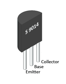
Transistor S9014 Pinout

S9014 Pinout

Electret condenser type microphone

Electret condenser microphone


If you have any confusion about capacitor value, check this.
Continue reading...

Measuring Milliohms with a Multimeter

Low values of resistance can be troublesome especially when large current s f low through them. A current of, say, 10 A passing through a terminal with a contact resistance of 50 m? will produce a voltage difference of 0.5 V. This resulting power loss of five watts is dissipated in the termination and can give rise to a dangerously high temperature which may degrade insulation around the wires.

Measuring Milliohms with a Multimeter Circuit Diagram

Measuring Milliohms with a Multimeter-Circuit Diagram

Measuring low values of resistance is not easy. Low cost multimeters do not include a milliohm measurement range and specialist equipment is expensive. The simple circuit described here allows milliohm measurements to be made safely on a standard ist equipment is expensive. The simple circuit described here allows milliohm measurements to be made safely on a standard multimeter. The circuit consists of little more than a 6 V voltage regulator and a mains adapter capable of supplying around 300 mA at 9 to 12 V.

The circuit supplies a fixed cur-rent output of 100 mA or 10 mA selected by switch S1. This connects either the 60 ? or 600 ? resistor into the constant current generator circuit. The resistor values are produced by paralleling two identical resistors; 120 ? and 1.2 k? from the E12 standard resistor range. Two test leads with probes are used to deliver current to the test resistance. The resultant voltage drop is measured by the multimeter (M1). With the test current set to100 mA a measurement of 1 mV indicates a resistance of 10 m?. At 10 mA (with S1 in the position shown in the diagram) a measurement of 1 mV indicates a resistance of 100 m? while 0.1 mV is equal to 1 m?. Diode D1 protects the meter from too high an input voltage.

With the voltmeter connected as shown in the diagram it measures not only the voltage drop across RX but also that produced by the resistance of the test leads, and probes. To make a true measurement, first touch the probes close together on the same lead of the test resistance and note the reading, now place the probes across the test resistance and note the reading again. The first reading measures just the test leads and probes while the second includes the resistance RX. Subtract the first measurement from the second to get the value of RX.

The accuracy of the measurements are influenced by the contact resistance of switch S1, the precision of resistors R1 to R4, the 6 V supply level and of course the accuracy of the measuring voltmeter. For optimum decoupling C1 should be fitted as close as possible to pin1 of IC1. An additional electrolytic capacitor of around 500 µF can be used at the input to the circuit if the input voltage from the AC power adapter exhibits excessive ripple.

Source:  http://www.ecircuitslab.com/2012/03/measuring-milliohms-with-multimeter.html
Continue reading...

13 8Vdc 2A Regulated Power Supply Circuit Diagram

This 13.8Vdc 2A Regulated Power Supply Circuit Diagram consists of step-down transformer Tl, a full-wave rectifier bridge (D1 through D4), and a filtering regulator circuit made up of Cl, C2, Rl, R2, R8, D5, and Ql, When 120 Vac is provided, the neon-lamp assembly LI lights up, and transformer Tl changes 120 Vac to about 28 Vac. 

The rectifier bridge, )1 through D4, rectifies the ac into pulsating dc, which is then filtered by Cl. Capacitor Cl acts as a storage capacitor. Zener diode 1)5 keeps the voltage constant across the base of Darlington regulator Ql, causing constant voltage across resistor R3 and the (+) and (-) output terminals, where the load is connected. Fuse F2 is used to open (blow), if the current through the output terminals is too high. Make sure to take proper precautions when using projects powered by 120 Vac.

 13.8Vdc 2A Regulated Power Supply Circuit Diagram


13.8Vdc 2A Regulated Power Supply Circuit Diagram

Continue reading...

SMD FM Transmitter

Let’s construct a low-power FM transmitter using surface-mount devices (SMD) that will be received with a standard FM radio. Soldering surface mounted devices is not so hard and actually is quite easy. There are many designs for small FM transmitters but they have some problems. First, you need an audio amplifier to get enough modulation. Second, the antenna is attached directly to the collector.

Third, the coil L must be wound by hand and adjusted by stretching. It all ads with a weak signal that tends to drift in frequency. In contrastm the transmitter schematic we present here eliminates some of those problems, using varactor diode for tuning and modulation, givind great sensitivity without an audio amplifier.


FM Transmitter – How it works

The figure below shows the schematic of the transmitter which consists of two stages: an oscillator and an output amplifier. Modulation is from an electret microphone but you can use a low power audio source.

Oscillator stage

Transistor Q1 is a Colpitts oscillator where the frequency is determined by the parallel resonant circuit formed by inductor L, varactor V1 and capacitors C7 and C8. Q1 is a common-collector amplifier where the power gain counts. V1 is actually a dual varactor that eliminate the possibility of forward conduction at the sinewave peaks.

The frequency of oscillation is set by adjusting the DC voltage on V1 with potentiometer R2. R4 and C3 form a low-pass filter to prevent RF from feeding back onto the DC. Capacitors C7 and C8 form an AC voltage divider to provide feedback at the emitter of Q1 to sustain oscillation. A necessary condition for oscillation to start is for the radio (C7+C8)/C7 to be sufficiently bigger than 1.

SMD transmitter circuit schematic


Frequency Modulation

Modulation is done by superimposing an audio signal from the electret mic onto the DC bias applied to V1. R3 and C1 form a low-pass filter to prevent RF from feeding back to the mic. R3, R4 and R2 form a votage divider for the audio.

Transmitter output stage

The output of the oscillator is fed through C9 to the Q2 emitter-follower. The output of Q2 drives the antenna through C11. The Q2 emitter-follower it ensures that the oscillator is not loaded down by the impedance of the antenna and it provides power gain to drive the antenna.

SMD Transmitter layout

The figure below shows the layout of the PCB and it uses surface-mounted devices like resistors and capacitors (non-polar devices). All the caps are size 0805 and all resistors are size 1206. use through-hole components for Q1, Q2, IC1 and V1. You can use an SOT-89 device for IC1 and an SOT-23 device for V1. Use MPSH10 or a transistor equivalent. Here you can learn how to solder smd chips.


The inductor

A coil would consist of two or three turns of wire but for this schematic we will use an inductor with loops of copper on the PCB. Such flat spiral inductor are common at these frequencies.
One formula for flat spiral inductors is:
flat spiral inductors formula where
L = inductance in uH
r = radius of coil (outer radius + inner radius divided by 2 ) inches
N = number of turns
d = depth of coil (outer radius minus inner radius) inches

Tuning range

While commercial FM band goes from about 88 MHz to 108 MHz, the L and C values used in this design allow tuning up to 100 MHz.

Transmitter testing

You will need a portable FM radio and an assistant. First, find an empty spot on the FM dial and set your radio about 30 feet away (9 meters). The radio’s volume control should not be set too high to prevend feedback. Next, power-up your transmitter and talk to yourself as you adjust the frequency with the trim-pot. When your assintant hears you, your transmitter is tuned. You might have to adjust the radio’s tuner slightly for best reception.

Have fun with it but remember that using the transmitter as a bugging device may not be legal in your country. To use the circuit as a wireless microphone, increase the value of R3. The transmitter range is about 100 feet (30 meters) inside a building.

Parts list

Continue reading...

Wednesday, December 18, 2013

The cell phone jammer company will celebrate its anniversary next month

The cell phone jammer company will celebrate its anniversary next month.
B, Java (Binary Runtime Environment for Wireless) game Java is a programming language, specifically what programming language we did not need to know. As a family game, we need to know two things: first, whether your cell phonesupports Java, to understand that you can access your phones manual or ask the dealer directly. Second, you choose whether to support a Java game for your mobile phone, to understand this, you can see "Why mobile game will have compatibility issues" and "how to download games from Sina for your cell phonemodel mobile cell phonegame" part of the . Here, there is a need to explain the misunderstanding that sometimes we talk about java games, often the first thought is probably the end of the cell phoneconfiguration, in fact, this is a big ideological errors. The factory inspection and acceptance personnel should sign the report of cell phone jammer if cell phone jammer is qualified.
Because the cell phoneis not a computer, "configuration" the word simply does not make sense for us. C, Brew and Java game similar, Brew (Binary Runtime Environment for Wireless) is a programming language. So the same, we do not know what Brew is to use Brew (Binary Runtime Environment for Wireless), you only need to know your cell phonecan support it. Currently, only CDMA (Code Division Multiple Access) mobile cell phoneonly support but at the same time, CDMA (Code Division Brew (Binary Runtime Environment for Wireless), Multiple Access) also supports Java, so in order to reduce costs, developers are still willing to choose the general Java-based game development. Therefore, Brew of the game is not a lot of support. cell phone jammer adopts anti-explosive and anti-removable shell of good sealing ability to prevent explosion, water and sun-burnt.
D, Uni-Java games Uni-Java is China Unicoms mobile cell phonejust to prepare for a new common development platform, Meet the group is still in development, there is no mobile phone-based Uni-java release. But in the near future, Uni-java is bound to be a weapon of China Unicom. E. mrp domestic mobile cell phonegame which consists of Sky Network Technology Co., Ltd. [Hangzhou] developed a lightweight virtual platform MINIJ platform format, using standard written in ANSI C. Because it is self-developed, so in addition to the Internet, "Ranger cabin" space station and the stream has a bit of hand-size travel community to provide these applications and external Web download method, the current mobile games mrp civil official website has more detail www. mrp123.cn).
Continue reading...

Quality Stereo Wireless Microphone or Audio Link

This stereo FM wireless microphone also makes a great quality audio link. We tested it to beyond 50 meters and it was rock solid. It’s certainly not the first wireless microphone we’ve ever published but this one is a little different. It’s stereo, providing surprisingly good quality sound. Second, it has a really good range. We tested it at well over 50m and it was still performing very well – noise-free, in fact – but at the time we couldn’t get our receiver any further away. So it’s likely to have even better range than that.

Complete Project:

main-quality-stereo-wireless-microphone-or-audio-link-circuit


quality-stereo-wireless-microphone-or-audio-link quality-stereo-wireless-microphone-or-audio-link-circuit

Its easy to build, requires very little setup... and its cheap! In fact, the low price might turn some people off, thinking its low quality. Try it - and be pleasantly surprised!

quality-stereo-wireless-microphone-or-audio-link-front

Third, it really is simple to build – the hard work (the transmitter module) is already done for you. It’s just a matter of assembling the microphone module, which contains the electret mics themselves, preamp and level controls, and soldering the transmitter module onto it, "piggy back" style.

FM Transmitter:

Finally, the transmitter module is crystal-locked, so you won’t have the drift probles of some earlier wireless microphones. And just in case you were wondering, that doesn’t mean the output is locked to one particular frequency – it has a nifty synthesis circuit built in to give you the choice of seven different frequencies between 106.7MHz and 107.7MHz.

On-board preset pots adjust the sensitivity of each channel to take into account mic differences or if you require different levels in each channel.

fm-transmitter-module-top-side-view

By the way, the transmitter module is quite capable of operating at line level if you want just a line level transmitter (eg, to feed an audio program around your home). Sensitivity is about 100mV. Oatley Electronics, who designed the kit, have the transmitter module available by itself if that’s what you’re after. But more on that anon.

fm-transmitter-module-bottom-side-view

Parts Layout:

parts-layout-quality-audio-link-circuit-diagram
parts-layout-of-quality-stereo-wireless-microphone-or-audio-link

You also have the choice of two power supply levels – 3-6V or 7-15V DC. The latter results in a lower current drain. The transmitter module also has a "5V out" rail to supply power to the preamp module.

Circuit Diagram:

quality-stereo-wireless-microphone-or-audio-link-circuit-diagram

Two electret microphone inserts are supplied in the kit. These can be soldered direct to the PC board to make it a fully self-contained project or they can be attached to the board via suitable lengths of mini shielded coax cable. A third option is to use "proper" microphones – they can be electret or dynamic types – but no provision has been made for plugging these in.

Typical Specifications: 
 
Audio response:.....................20Hz-15kHz.
Channel separation: ........................40dB
Total Harmonic Distortion: ...............0.1%
Output Frequency:...........106.7-107.2MHz
Pre Emphasis: ..................................50μS
DC supply voltage range: ................3-15V
Supply Current: .......................30mA @ 9V
Source: http://www.ecircuitslab.com/2011/06/quality-stereo-wireless-microphone-or.html
Continue reading...

A good business is not really the appreciation

 A good business is not really the appreciation of the work and marketing tool received suffering from markets and telephone product of the strength is the key to victory, of course, low comprehensive

listing of G808 last year continue to allow me to appreciate the dance of the Samsung. It is the process and result of performing every operational instruction of

cell phone jammer .
The replacement phone of HTC product cycle is very fast, almost did not take long on a machine Huang. HTC family of Windows machines Huang HTC HD3, do not know yet listed. While Android is in fact

the front is not long, nothing more than the G3, the Hero. I think for many people, especially Chinese people do not want to play the machine to send messages to call you taking pictures, do not

buy the HTC. If you have a business role, the entertainment capital of the class you want to see the movie, send email, browse the World Wide Web, play a large 3D games. Then you consider that HTC

well. The most important thing is that the HTC machine hardware configuration is very good, and that old-fashioned Nokia is completely different. To show the detailed status of

cell phone jammer .
I saw a little boy says: Im gay, I use the M8 - and then immediately replied: do not lose our gay face on the cnbeta. Now is not a phone as small as possible. You go to Europe and the United

States to take a look at those famous models, they go on the street holding his hands a large mobile phone to send text messages there. Looks super Fan children. - Suitable for girls with Sharp a

lot of heads are not small, is said to hand a small little girls no way to single-handedly control the Sharp. I phone is very large, two hands to get maintained, BlackBerry texting should at least

use two hands. - On the trend of mobile phones the size of argument, I am more biased in favor of mobile phone now or bigger only decent. The system administrator can screen cell phone jammer .
Millet mobile marketing strategies and models dismantling. Presentation online site finishing. Introduction: the popularity of millet phone and the millet mobile phone marketing strategy is

inseparable from millet phones with what kind of marketing strategy?
Continue reading...

Bass Treble Controller Using 741 Op Amp

This is simple but powerful bass, treble, volume control is made by General Op-Amp IC LM741. The input voltage is 12V, but it will also work with 9V and 6V. This has inbuilt pre-amplifier also. Left channel is shown. Right channel is same.

Low Cost Bass-Treble Controller Using Op-Amp 741

Parts List:

IC LM741 x1
T/C 10k,22k,100k All x1
Triansistor BC148/548 = 1
220uF/25V = 2
4.7uF/25V = 2
2.2uF/10V = 1
10uF/25V = 1
Small resistors x12p
Small PF x5p
Continue reading...

Solar Cell Voltage Regulator

This device is designed to be a simple, inexpensive ‘comparator’, intended for use in a solar cell power supply setup where a quick ‘too low’ or ‘just right’ voltage indicator is needed. The circuit consists only of one 5V regulator, two transistors, two LEDs, five resistors, two capacitors, and one small battery. Although a 4-V battery is indicated, 4.5 V (3 alkalines in series) or 3.6 V (3 NiCd cells in series) will also work.

The specifications of voltage regulator IC1 are mainly determined by the size and number of the solar cells and the current pull of the equipment connected to the output. Here the low-drop 4805 is suggested but other regulators may work equally well as long as you observe the output voltage of the solar cells. Transistors T1 and T2 are complementary types i.e. one each of the pnp and npn variety.

Circuit diagram:
solar cell voltage regulator circuit schematic
Solar Cell Voltage Regulator Circuit Diagram

Although the ubiquitous BC557B (pnp) and BC547B (npn) are indicated, any small-signal equivalents out of the junk box will probably do. The values of voltage dividers R1/R6 and R3/R4 may need to be adjusted according to the type of transistor and its gain, or according to the desired voltage thresholds. Using the resistor values shown in the schematic, LED D2 turns on fully when the voltage is just above 5 volts.

LED D1 turns on when the voltage drops below 4.2 volts or so. Between those two thresholds, there is a sort of no man’s land where both LEDs are on dimly. A buzzer or other warning device could be connected across the terminals of LED D1 to give a more substantial warning if the voltage drops below operating limits. The current consumption of the circuit is about 20 mA at 5 V, and it decreases with the voltage supplied by the solar cells.
Reuben Posthuma
Continue reading...

Tuesday, December 17, 2013

Soft Start For Switching Power Supply

Switching power supply whose output voltage is appreciably lower than its input voltage has an interesting property: the current drawn by it is smaller than its output current. However, the input power (UI) is, of course, greater than the output power. There is another aspect that needs to be watched: when the input voltage at switch-on is too low, the regulator will tend to draw the full current.

When the supply cannot cope with this, it fails or the fuse blows. It is, therefore, advisable to disable the regulator at switch-on (via the on/off input). until the relevant capacitor has been charged. When the regulator then starts to draw current, the charging current has already dropped to a level which does not overload the voltage source.

Circuit diagram:

Soft Start Circuit Diagram For Switching Power Supply

Soft Start Circuit For Switching Power Supply

The circuit in the diagram provides an output voltage of 5 V and is supplied by a 24 V source. The regulator need not be disabled until the capacitor is fully charged: when the potential across the capacitor has reached a level of half or more of the input voltage, all is well. This is why the zener diode in the diagram is rated at 15 V. Many regulators produced by National Semiconductor have an integral on/off switch, and this is used in the present circuit.

The input is intended for TTL signals, and usually consists of a transistor whose base is accessible externally. This means that a higher switching voltage may be applied via a series resistor: the value of this in the present circuit is 22 kΩ. When the voltage across the capacitor reaches a level of about 17 V, transistor T1 comes on, whereupon the regulator is enabled.
Source: National Semiconductors
Continue reading...

The trial run of production of cell phone jammer

 The trial run of production of cell phone jammer has been finished.
The nature of the system parameters and target system performance impact of airborne laser scanning system in the ranging process, the scanning angle is continuous change, Air to bring scattering scattering echo intensity is closely related to the scan angle, the echo power nadir Air band edge minimum SNR of the system and ranging accuracy and scanning angle, the flight strip 13 the edge of the ranging accuracy in the field of view angle is too large, have to exceed the system allow ranging accuracy range. On the other hand, vary greatly due to the reflectance of ground targets, the reflectivity of the target largely determines the echo intensity, so that it could cause some surface features not receive echo In particular, the band edge in the Air. It is during the technology discussion meeting of phone jammer .The customer can know the design or technology of mobile phone jammer  in advance
Therefore, for a practical system, the flying height and scan angle should be an allowed range, necessary for the flying height, scan angle, the system parameters and surface reflectance impact on system performance for in-depth theoretical study. 9.5 data classification and identification to obtain the raw data first has to go through gross error detection, and then create a ground-based data types, separation of non-ground data, based on customer requirements, non-ground data classification, such as building class data, and transmission line data, railroads data, simply use the distance data of the laser radar or laser reflection intensity information classification and identification of surface features is not satisfactory, we can not play the advanced nature of the laser radar technology. It is the design revise of phone jammer . 
 LVL 8 Dalian Economic and Technological Development Zone Laser Technology Development Co., Ltd. Dalian Economic and Technological Development Zone Lats Laser Technology Development Co., Ltd. Economic and Technological Development Zone JZC-G manual. Maintenance and annual inspection of the JZC 6.1 JZC of Maintenance maintenance period JZC maintenance period, such as instrument quality, free repair by the company responsible, and bear the shipping costs after repair, such as damage caused by improper, I am responsible for repairs, and collect the parts Gongben fee. Maintenance in the maintenance of more than maintenance of equipment problems, responsible for the repair will be based on the maintenance of price by us alone. The visual inspection should be done for the quality inspection of phone jammer .
Continue reading...

Full duplex Intercom

No complex switching required, Simple circuitry, 6-12V supply
This design allows to operate two intercom stations leaving the operator free of using his/her hands in some other occupation, thus avoiding the usual "push-to-talk" operation mode. No complex changeover switching is required: the two units are connected together by means of a thin screened cable. As both microphones and loudspeakers are always in operation, a special circuit is used to avoid that the loudspeaker output can be picked-up by the microphone enclosed in the same box, causing a very undesirable and loud "howl", i.e. the well known "Larsen effect". A "Private" switch allows microphone muting, if required.
Circuit Diagram :
Full-duplex Intercom Circuit diagram Full-duplex Intercom Circuit diagram
Parts:
P1_____________22K Log. Potentiometer
R1_____________22K 1/4W Resistor
R2,R3_________100K 1/4W Resistors
R4_____________47K 1/4W Resistor
R5______________2K2 1/4W Resistor (See Notes)
R6______________6K8 1/4W Resistor
R7_____________22K 1/2W Carbon or Cermet Trimmer
R8______________2K7 1/4W Resistor
C1,C6_________100nF 63V Polyester or Ceramic Capacitors
C2,C3__________10µF 63V Electrolytic Capacitors
C4_____________22µF 25V Electrolytic Capacitor
C5_____________22nF 63V Polyester or Ceramic Capacitor
C7____________470µF 25V Electrolytic Capacitor
Q1____________BC547 45V 100mA NPN Transistor
IC1_________TDA7052 Audio power amplifier IC
SW1____________SPST miniature Switch
MIC____________Miniature electret microphone
SPKR___________8 Ohm Loudspeaker
Screened cable (See Text)
Circuit operation:
The circuit uses the TDA7052 audio power amplifier IC, capable of delivering about 1 Watt of output power at a supply voltage comprised in the 6 - 12V range. The unusual feature of this design is the microphone amplifier Q1: its 180° phase-shifted audio output taken at the Collector and its in-phase output taken at the Emitter are mixed by the C3, C4, R7 and R8 network and R7 is trimmed until the two incoming signals almost cancel out. In this way, the loudspeaker will reproduce a very faint copy of the signals picked-up by the microphone.
At the same time, as both Collectors of the two intercom units are tied together, the 180° phase-shifted signal will pass to the audio amplifier of the second unit without attenuation, so it will be loudly reproduced by its loudspeaker. The same operation will occur when speaking into the microphone of the second unit: if R7 will be correctly set, almost no output will be heard from its loudspeaker but a loud and clear reproduction will be heard at the first unit output.
Notes:
  • The circuit is shown already doubled in the diagram. The two units can be built into two separate boxes and connected by a thin screened cable having the length desired.
  • The cable screen is the negative ground path and the central wire is the signal path.
  • The power supply can be a common wall-plug adapter having a voltage output in the 6 - 12V dc range @ about 200mA.
  • Enclosing the power supply in the box of one unit, the other unit can be easily fed by using a two-wire screened cable, its second wire becoming the positive dc path.
  • To avoid a two-wire screened cable, each unit may have its own separate power supply.
  • Please note that R5 is the only part of the circuit that must not be doubled.
  • Closing SW1 prevents signal transmission only, not reception.
  • To setup the circuit, rotate the volume control (P1) of the first unit near its maximum and speak into the microphone. Adjust Trimmer R7 until your voice becomes almost inaudible when reproduced by the loudspeaker of the same unit.
  • Do the same as above with the second unit.
Source :  http://www.ecircuitslab.com/2011/06/full-duplex-intercom-circuit.html
Continue reading...

LED Sound level display circuit by using IC LM3915

This circuit is about audio sound level LED display, indicator, monitor or you can say it “Audio VU (Volume Unite) Meter”.
This is a simple audio sound level LED display circuit diagram. The circuit is completely  based on  a single ic LM3915 from National Semiconductor. The LM3915 is a monolithic integrated circuit. It displays the audio sound level in terms of 10 LEDs and providing a logarithmic 3 dB/step analog display.

Audio sound level display circuit diagram


Fig: Circuit diagram of sound level display using ic LM3915
The audio sound level LED display circuit can operate from a single supply 3V to 25V. But I  suggest to use 9-12V. LED brightness can be controlled with a single pot( variable resistor) as shown 10K ohm in the circuit. Connect the audio input signal in Pin-5 of LM3915 from output of a audio device like output of audio amplifier or any other source.
The Pin-9 of LM3915 is to select dot or bar mode display. To make the circuit moving dot display instead of a bar graph display disconnect the Pin-9 from +V.
Continue reading...

The GPS mobile phone jammer owns the slow start circuit design

The GPS mobile phone jammer owns the slow start circuit design.
As the profit margins of the conflict, the downstream distributors that upstream channel or production companies to earn more profits. There are channels of bargaining ability, regardless of the level of the channel members, as long as it is gradually expanding their own market power, more resources and profits from the upstream and downstream enterprises, resulting in a conflict. Compensate for price cuts, promotional costs and defective products and services is often a lot of conflict. Competitor analysis 1.3.1 Motorolas channel strategy for Motorolas channel has mainly taken the form of agency. Its development can be divided into several stages: before 1995, subject to the constraints of the market environment, Motorola sold by China Telecom. The power supply switch of GPS mobile phone jammer will generate the powerful current.
In 2002, Nokia strengthened at the retail level to compete with Motorolas comprehensive attempt selected five major chain stores in Shanghai and Guangdong, as a direct supply store. Across the agents directly to their supplier. In addition, in many provinces, Nokia in the seven major real estate agents outside a few strong regional distributors as a proxy to participate in the distribution of several models to compensate for the lack of agents across the country (Figure ). At the same time in the national underwriting way in some provinces and gradually try to regional underwriting. Nokia to enter the Chinese market than Motorolas much shorter time, so not much of a burden, distributors conditional direct construction of sales network. The effective shielding range of GPS mobile phone jammer is 5-10m.
Postel mainly rely on an agent on the market, such as long-term, Capitel Nokia store in major cities to establish system. Another feature of the Nokia channel construction is authorized service center functions with the store to play the store after-sales service advantages. From the characteristics of channel management, Nokias overall policy of the channel members are: multi-channel, few links, network refinement, price transparency. Nokia has recognized the phone as early as the end of 1997, will soon become a mature and transparent products, does not hold too many levels in the supply chain, develop and implementation of the Retail Management Plan is now store / concession counters plan. The rechargeable power supply of GPS mobile phone jammer is AC110-250V.The actual shielding range of mobile phone jammer is in the place
Continue reading...

Monday, December 16, 2013

Motorcycle Battery Monitor Circuit Diagram

A circuit for monitoring the status of the battery and generator is undoubtedly a good idea for motorcyclists, as for other motorists. However, not every biker is willing to drill the necessary holes in the cockpit for the usual LED lamps, or to screw on an analogue accessory instrument. The circuit shown here manages to do its job with a single 5-mm LED, which can indicate a total of six different conditions of the onboard electrical system. This is done using a dual LED that can be operated in pulsed or continuous mode (even in daylight). Built on a small piece of prototyping board and fitted in a mini-enclosure, the complete circuit can be tucked inside the headlamp housing or hidden underneath the tank.
  Motorcycle_Battery_Monitor_Circuit_Diagram01
The heart of the circuit is IC2, a dual comparator. The comparator circuit is built without using any feedback resistors, with the indication being stabilised by capacitors C4 and C5 instead of hysteresis. Small 10-µF tantalum capacitors work well here; 220-µF ‘standard’ electrolytic capacitors are only necessary with poorly regulated generators. Voltage regulator IC1 provides the reference voltage for IC2 via voltage divider R2/R3. The onboard voltage is compared with the reference voltage via voltage dividers R4 /R5 and R6/R7, which are connected to the inverting and non-inverting comparator sections, respectively.
PSU_Table_Motorcycle_Battery_Monitor_Circuit_Diagram02
Using separate dividers allows the threshold levels to be easily modified by adjusting the values of the lower resistors. IC2a drives the anode of the red diode of LED D4 via pull-up resistor R10. The anode of the green diode is driven by IC2b and R11. T2 pulls R11 to ground, thereby diverting the operating current of the green diode of the LED, if the voltage of the electrical system exceeds a threshold level of 15 V (provided by Zener diode D3). The paralleled gate outputs on pins 10 and 11 of IC3 perform a similar task. However, these gates have internal current limiting, so they can only divert a portion of the current from the red diode of the LED.
Table_Motorcycle_Battery_Monitor_Circuit_Diagram3
The amount of current diverted depends on the battery voltage. The two gates are driven by an oscillator built around IC3a, which is enabled via voltage divider R14/R15 and transistor T1 when the battery voltage is sufficiently high. Depending on the state of IC3a, the red diode of the LED blinks or pulses. The circuit is connected to the electrical system via fuse F1 and a low-pass filter formed by L1 and C1. If you cannot obtain a low-resistance choke, a 1-Ω resistor can be used instead. In this case, the values of C3, C4 and C5 should be increased some-what, in order to help stabilise the indication. D1 protects the circuit against negative voltage spikes, as well as offering protection against reverse-polarity connection. Due to its low current consumption (less than 30 mA), the circuit could be connected directly to the battery, but it is better to power it from the switched positive voltage.

Source :  http://www.ecircuitslab.com/2011/08/motorcycle-battery-monitor-circuit.html
Continue reading...

Thursday, October 10, 2013

Clap Switch Circuit Diagram

Here’s a clap switch free from false triggering. To turn on/off any appliance, you just have to clap twice. The circuit changes its output state only when you clap twice within the set time period. Here, you’ve to clap within 3 seconds. The clap sound sensed by condenser microphone is amplified by transistor T1. The amplified signal provides negative pulse to pin 2 of IC1 and IC2, triggering both the ICs. IC1, commonly used as a timer, is wired here as a monostable multivibrator. Trigging of IC1 causes pin 3 to go high and it remains high for a certain time period depending on the selected values of R7 and C3. This ‘on’ time (T) of IC1 can be calculated using the following relationship: T=1.1R7.C3 seconds where R7 is in ohms and C3 in microfarads. On first clap, output pin 3 of IC1 goes high and remains in this standby position for the preset time.Also, LED1 glows for this period. The output of IC1 provides supply voltage to IC2 at its pins 8 and 4.
Circuit diagram :
Clap Switch  Circuit Diagram
Now IC2 is ready to receive the triggering signal. Resistor R10 and capacitor C7 connected to pin 4 of IC2 prevent false triggering when IC1 provides the supply voltage to IC2 at first clap. On second clap, a negative pulse triggers IC2 and its output pin 3 goes high for a time period depending on R9 and C5. This provides a positive pulse at clock pin 14 of decade counter IC 4017 (IC3). Decade counter IC3 is wired here as a bistable. Each pulse applied at clock pin 14 changes the output state at pin 2 (Q1) of IC3 because Q2 is connected to reset pin 15. The high output at pin 2 drives transistor T2 and also energizes relay RL1. LED2 indicates activation of relay RL1 and on/off status of the appliance. A free-wheeling diode (D1) prevents damage of T2 when relay de-energizes.
Author : Mohammad Usman Qureshi - Copyright : Electronics For You May 2003
Continue reading...

1998 Ford f800 Wiring Diagram

1998 Ford f800 Wiring Diagram
(click for full size image)

The Part of 1998 Ford f800 Wiring Diagram: power distribution, indicator, air switch, switch closed, diesel, switch testing, buzzer module, engine alarm, stihes.
Continue reading...

Wednesday, October 9, 2013

Grand Prix Starting Lights

This circuit reproduces the starting light sequence currently used by FISA for Formula One racing. It could be used with slot car sets (such as HO scale AFX/Life Like/Tyco sets) or radio controlled cars. IC1, a 555 timer IC, is used as a clock pulse generator. Its output is fed via NAND gates IC2a and IC2c to IC3, a 4024 binary counter. IC2b inverts the O4 output of 4024 binary counter IC3. Initially, IC3 is reset and all its outputs are low, including O4, which causes IC2b to present a logical high to the pin 8 input of IC2c which then passes pulses from the 555 clock circuit to the clock input of the 4024. IC3 then begins counting.

After the count has reached binary 1111, the next pulse sends the O4 output of IC3 high, which disables IC2c and IC3 stops counting. The four used outputs of IC3 are connected to a resistor ladder which acts as a simple digital to analog convert-er (DAC). As the count increases so does the voltage produced at the top of the ladder and this is connected to the inverting inputs of four comparators inside IC4 (an LM339) and to IC5, which is a 741 op amp also connected as a comparator.

Grand Prix starting lights circuit schematic

The positive inputs of the comparators are connected to the taps of a voltage divider, with the tapping voltages set using VR1, a 100kO trimpot. As IC3 counts, the rising stepped voltage from the DAC ladder switches the comparators on in sequence, starting with IC4d and working up to IC5. As each comparator is turned on, its pair of LEDs is lit; first LEDs 1 & 2, then LEDs 3 & 4 and so on. When all five pairs of LEDs are lit, the next pulse from IC1 moves the binary count of IC3 to 10000, so the DAC voltage drops back to zero and all LEDs are extinguished. At the same time, counting also stops, because the high on O4 causes IC2c to block further gate pulses. The circuit then remains inactive until the counter is reset by pressing push-button switch S1. This allows a new sequence to begin.
Continue reading...

1971 Ford Half Ton Wiring Diagram

1971 Ford Half Ton Wiring Diagram


The Part of 1971 Ford Half Ton Wiring Diagram: direct switch, high beam, right headlight, horn relay,
green wire, indicator, fusible link, battery, starter relay, egr system, left marker light, ignition module, distributor, yellow wire, alternator indicator, washer fuse, windshield wiper switch, regulator,
Continue reading...

Cheap Switch Mode DC DC Converter

This circuit is based on mobile phone chargers. These chargers are based on the Motorola MC34063 switch-mode IC. By changing the values of the feedback resistors (R1 & R2), the output voltage can be varied over a wide range. Just modify R1 and R2 according to the formula: Vout = 1.25 (1+R2/R1). The values shown give an output of 3V.

Cheap Switch-Mode DC-DC Converter circuit schematic
Continue reading...

Lead Acid Battery Charger 2

The above pictured schematic diagram is just a standard constant current model with a added current limiter, consisting of Q1, R1, and R4. The moment too much current is flowing biases Q1 and drops the output voltage. The output voltage is: 1.2 x (P1+R2+R3)/R3 volt. Current limiting kicks in when the current is about 0.6/R1 amp. For a 6-volt battery which requires fast-charging, the charge voltage is 3 x 2.45 = 7.35 V. (3 cells at 2.45v per cell). So the total value for R2 + P1 is then about 585 ohm. For a 12 V battery the value for R2 + P1 is then about 1290 ohm. For this power supply to work efficiently, the input voltage has to be a minimum of 3V higher than the output voltage. P1 is a standard trimmer potentiometer of sufficient watt for your application. The LM317 must be cooled on a sufficient (large) coolrib. Q1 (BC140) can be replaced with a NTE128 or the older ECG128 (same company). Except as a charger, this circuit can also be used as a regular power supply.

Lead Acid Battery Charger circuit diagramParts List:

R1 = 0.56 Ohm, 5W, WW
R2 = 470 Ohm C2 = 220nF
R3 = 120 Ohm
R4 = 100 Ohm
C1 = 1000uF/63V
Q1 = BC140
Q2 = LM317, Adj. Volt Reg.
C3 = 220nF (On large coolrib!)
P1 = 220 Ohm
Continue reading...

Balanced Output Board For The Stereo DAC

balanced-output-board-for-the-stereo-dac-cicuitw

This add-on board is designed to provide a pair of balanced audio outputs for the High-Quality Stereo DAC (Digital to Analog Converter). Two 3-pin male XLR connectors are used for the new outputs and they can either replace or augment the existing unbalanced outputs without affecting their performance. Balanced audio is used in recording studios and on stage because of its improved noise immunity.

Picture of the project:

  balanced-output-board-for-the-stereo-dac-cicuit-schematicw  

This is due to the fact that the signal is sent differentially (ie, as two signals 180° out of phase) and then converted to a single-ended voltage signal at the far end. If any noise is picked up in the cable, it affects the two out-of-phase signals equally so that when the signals are subsequently subtracted, most of the noise is eliminated.

Parts layout:

parts-layoutbalanced-output-board-for-the-stereo-dacw

In addition, the DAC’s performance at the balanced outputs generally exceeds that of the unbalanced outputs, although only by a small margin. The signal-to-noise ratio, frequency response and channel separation are all better, although we measured a tiny bit more distortion from the balanced outputs. However, both levels are so low as to be almost negligible.

Circuit diagram:

balanced-output-board-for-the-stereo-dac-cicuit-diagramw

Comparison chart:

chart tabl


Source : www.siliconchip.com

Continue reading...