Showing posts with label a. Show all posts

Wednesday, November 12, 2014

Build Power Amplifier LM3876 Simply and Powerfull Power Amplifier

The chip on which the amplifier is based, a Type LM3876, is a member of the Overture family from National Semiconductor, All members of this family are pin-compatible and mutually interchangeable. They are typified by an internal protection (called SPIKE). In practice, the diftection ference between them is the power output. The series was described on the basis of the LM3886 in an earlier issue*.

The PCB has been designed so what it can accommodate the LM3876 (50W) as well as the LM3886 (150W). Because of this, pin5 of the IC on the board is connected to the positive supply line. This connection is not needed for the LM3876, since its pin5 is not (internally) connected (NC).

The IC is located at the side of the board to facilitate fitting it to a heat sink as shown in the photograph.

An important aspect for optimum performance is the decoupling of the unregulated supply lines by C 7-10. All earth connections go to a single terminal on the board.

Air-cored inductor L1 consists of 13 turns of 1mm dia. enamelled copper wire with an inner diameter of 10mm. The completed inductor is pushed over R7 and its terminals soldered to those of the resistor.

All electrolytic capacitors must be mounted upright. The amplifier can be muted with a single-pole switch connected to the MUTE input (pin8). This function is enabled when the switch is open. If muting is not required, solder a wire bridge across the mute terminals on the board.

Boucherot network R6-C6 is not normally required in this application, but provision has been made for it for use in other applications.

According to the manufacturers, both chips are optimalized for a load of 8 Ohm. The output power is lower when a 4 Ohm load is used or when the supply voltage is reduced. When a 4 Ohm load is used, the SPIKE protection becomes active when the supply voltage is about 27V, resulting a in a reduction of the power output to 10W. This means that it is not advisable to use loudspeaker with an impedance <8 ohm.

For best result you can expand power amplifier using BPA-200 Amplifier


Part listResistor:
R1, R3 = 1 k
R2, R4, R5 = 18k
R6 = see text
R7 = 10R, 5 Watt
R8, R9 = 22k

Capacitors:
C1 = 2.2 uF
C2 = 220 uF, 160 V
C3 = 22 uF, 40 V
C4 = 47 pF
C5 = 100 uF, 40 V
C6 = see text
C7, C8 = 100 nF
C9, C10 = 1000 uF, 40 V

Inductors:
L1 = 0.7 uH - see text

Integrated circuits:
IC1 = LM3876T

Miscellaneous:
Heat sink for IC1 <1.5 k w-1
Single-pole switch - see text


Schematic and PCB Layout LM3876
Continue reading...

Tuesday, November 11, 2014

A Hiqh Quality Headphone Amplifier Schematic

Some lovers of High Fidelity headphone listening prefer the use of battery powered headphone amplifiers, not only for portable units but also for home "table" applications. This design is intended to fulfill their needs. An improved output driving capability is gained by making this a push-pull Class-B arrangement. Output power can reach 100mW RMS into a 16 Ohm load at 6V supply with low standing and mean current consumption, allowing long battery duration.

Circuit diagram:
 a high quality headphone amplifier schematic circuit diagram
High Quality Headphone Amplifier Circuit Diagram


Parts:Resistors:
P1 = 22K Potentiometer
R1 = 15K Resistor
R2 = 100K Resistor
R3 = 100K Resistor
R4 = 47K Resistor
R5 = 470R Resistor
R6 = 500R Resistor
R7 = 1K Resistor
R8 = 18K Resistor
R9 = 18K Resistor
R10 = 2.2R Resistor
R11 = 2.2R Resistor
R12 = 33R Resistor
R13 = 4.7K ResistorCapacitors:
C1 = 10uF-25V Capacitors
C2 = 10uF-25V Capacitors
C3 = 100nF-63V (PF)
C4 = 220uF-25V Capacitors
C5 = 100nF-63V (PF)
C6 = 220uF-25V CapacitorsSemiconductors:
Q1 = BC560C PNP Transistor
Q2 = BC560C PNP Transistor
Q3 = BC550C NPN Transistor
Q4 = BC550C NPN Transistor
Q5 = BC560C PNP Transistor
Q6 = BC327 PNP Transistor
Q7 = BC337 NPN TransistorMiscellaneous:
J1 = RCA Audio Input Socket
J2 = 3mm Stereo Jack Socket
B1 = 6V Battery Rechargeable
SW1=SPST Slide or Toggle Switch

Notes:
  • For a Stereo version of this circuit, all parts must be doubled except P1, SW1, J2 and B1.
  • Before setting quiescent current rotate the volume control P1 to the minimum, Trimmer R6 to maximum resistance and Trimmer R3 to about the middle of its travel.
  • Connect a suitable headphone set or, better, a 33 Ohm 1/2W resistor to the amplifier output.
  • Switch on the supply and measure the battery voltage with a Multimeter set to about 10Vdc fsd.
  • Connect the Multimeter across the positive end of C4 and the negative ground.
  • Rotate R3 in order to read on the Multimeter display exactly half of the battery voltage previously measured.
  • Switch off the supply, disconnect the Multimeter and reconnect it, set to measure about 10mA fsd, in series to the positive supply of the amplifier.
  • Switch on the supply and rotate R6 slowly until a reading of about 3mA is displayed.
  • Check again the voltage at the positive end of C4 and readjust R3 if necessary.
  • Wait about 15 minutes, watch if the current is varying and readjust if necessary.
  • Those lucky enough to reach an oscilloscope and a 1 KHz sine wave generator can drive the amplifier to the maximum output power and adjust R3 in order to obtain a symmetrical clipping of the sine wave displayed.


Technical data:Output power (1 KHz sine wave):
  • 16 Ohm: 100mW RMS
  • 32 Ohm: 60mW RMS
  • 64 Ohm: 35mW RMS
  • 100 Ohm: 22.5mW RMS
  • 300 Ohm: 8.5mW RMS
Sensitivity:
  • 160mV input for 1V RMS output into 32 Ohm load (31mW)
  • 200mV input for 1.27V RMS output into 32 Ohm load (50mW)
Frequency response @ 1V RMS:
  • Flat from 45Hz to 20 KHz, -1dB @ 35Hz, -2dB @ 24Hz
Total harmonic distortion into 16 Ohm load @ 1 KHz:
  • 1V RMS (62mW) 0.015% 1.27V RMS (onset of clipping, 100mW) 0.04%
Total harmonic distortion into 16 Ohm load @ 10 KHz:
  • 1V RMS (62mW) 0.05% 1.27V RMS (onset of clipping, 100mW) 0.1%
  • Unconditionally stable on capacitive loads
Continue reading...

Thursday, October 30, 2014

MAKING A ZENER DIODE

Sometimes a zener diode of the required voltage is not available. Here are a number of components that produce a characteristic voltage across them. Since they all have different voltages, they can be placed in series to produce the voltage you need. A reference voltage as low as 0.65v is available and you need at least 1 to 3mA through the device(s) to put them in a state of conduction (breakdown).


source : http://www.talkingelectronics.com.au/projects/200TrCcts/200TrCcts.html
Continue reading...

Thursday, October 16, 2014

Build a Bass Treble Tone Control Circuit Diagram

How build a Bass-Treble Tone Control Circuit Diagram . The LM1036 is a DC controlled tone (bass/treble), volume and balance circuit for stereo applications in car radio, TV and audio systems. An additional control input allows loudness compensation to be simply effected. Four control inputs provide control of the bass, treble, balance and volume functions through application of DC voltages from a remote control system or, alternatively, from four potentiometers which may be biased from a zener regulated supply provided on the circuit. Each tone response is defined by a single capacitor chosen to give the desired characteristic.

 Build a Bass-Treble Tone Control Circuit Diagram


Features:
  • Wide supply voltage range, 9V to 16V
  • Large volume control range, 75 dB typical
  • Tone control, ±15 dB typical
  • Channel separation, 75 dB typical
  • Low distortion, 0.06% typical for an input level of 0.3 Vrms
  • High signal to noise, 80 dB typical for an input level of 0.3 Vrms
  • Few external components required
Note:
Vcc can be anything between 9V to 16V and the output capacitors are
10uF/25V electrolytic.

Continue reading...

Thursday, September 25, 2014

Making a Homemade Large TV Projector Screen Home Theater System

If you are looking for a new hobby, here is a project which is exciting and yet so easy to construct. Imagine inviting your guests to watch the next foot ball world championship on your home theater from a small TV.

The thing which can make this possible is a lens called frensel lens.


Construction of the projector unit

The projector can be made from almost any material, cardboard being the easiest to work with. It is advisable to l make the first construction with cardboard and, after gain- ing confidence, the final case may be made of wood or decorative boards. The projector is built as shown in Fig. 1. The inside measurements A and B correspond to width and height respectively of the TV screen, the depth, is 48.25 cm and is the same for all sizes of TV sets. The rear of the case remains open. The front has a square opening where the-objective unit will slide in. The case can be made more stable by using good adhesive and masking tape around the corners and angles. Stability of the case is very important. The square opening D x D should be 30.5 cm x 30.5 cm for all TV sets above and up to 33 cm screen size.


Objective unit

This is made of same material as the projector unit. Here the front is open while the rear carries the lens. The wall thickness of the projector unit should be such that one should be able to slide this objective unit easily and horizontally, yet not so loose that it gets tilted in the square opening of the projector unit. The length E of the objective unit is 22.9 cm. The lens carrying sheet has a 14.6cm diameter hole in the center ( Fig. 1). Tape the special fresnel lens over this hole. Make sure you tape the edge of the lens only and not on the grooves as this will affect the clarity of the picture. The grooves on the lens, should always face towards the objective unit. When pushed into the projector, the grooved side should face the TV screen.  


Mirror

 Though the lens will magnify the TV picture, it will be inverted. lf the picture is vertically inverted, placing the TV set upside down can be avoided in the following manner:

I. Turn the deflection coil at the neck of the picture tube by 180 degree.

2. Alternatively, invert the terminals of the vertical and horizontal deflection coils through a slide switch as per the connection plan in Fig. 2; This will allow you to see the picture projected on giant screen or, by removing the projector unit, normally on TV by simply sliding the switch either way·as desired. If you have a 33cm transistorised portable set, ideal for  projection sharpness, you can turn the set upside down as this will not damage the set anyway. lf the picture is inverted side wise it can be remedied by inverting the vertical deflection coils. As an alternate method a mirror can be used. The mirror of 30.5 cm x 30.5 cm in size should be fixed on the projector mounting plate with the help of a mirror holder. The mirror  holder is easily made by using two wooden planks of l .27 cm x 5 cm x 30.5 cm each and fixing them at the mirror edge by contact adhesive. Now the mirror can stand vertically. The mirror should stand vertically making 450 angle to the lens. The light path through the TV projector is shown in Fig. 3. Final fixing of the mirror holder and the projector unit on a board should be done only after the final adjustments fora good. picture have been made.


Final construction

 After adjusting the TV set to obtain an upright picture,  bring the projector unit exactly in front of the TV screen. Use a supporting board of proper size and height for resting} the projector unit. Slide in the objective unit with the lens turned inside towards the TV screen and the grooved side of the lens facing the TV screen. Thereafter, place the big projector screen about 1.4m  away from, the projector, shutting off the room lights or external lights completely. Picture will be very bright only when the room is fully dark as in a cinema. Adjust the objective unit by sliding until a very sharp picture is projected on the screen. Now the screen can be moved back and forth and the objective unit adjusted again until the desired size and sharpness are obtained.

 very important point may be mentioned here. The brightness of the picture will depend on the reflective power, of the projector screen. The screen should be straight without any curve anywhere on its surface. Its bright white surface should be light reflecting type, not light-absorbing. For this reason Kodak’s Ektalit screen has been found to give picture so bright that it could be viewed even in a half-dark room.

In case of non-availability of this material similar results can be achieved by trying out small size (about 30.5 cm x 30.5 cm) smooth surfaces of different materials and painting them with different types of bright white paints. The one that gives the brightest picture can then be selected. Fix everything after the final adjustment. To give it a professional look, a black stripe can be painted on the screen to border the picture size. Allow little time to let your eyes get used to the darkness and enjoy your home cinema. To make it a realistic home cinema, an extra loudspeaker box can be placed behind the projector screen. The outside loudspeaker box and the TV loudspeaker can be easily connected in `either-or’ manner by means of a three pole jack or a slide switch. All these new switches can be fitted together on a small case or even built into the TV case. The inside walls of both objective and projector cases should be painted matt black to arrest diffused light and thereby obtain extra sharpness for the projected picture




Continue reading...

Friday, June 6, 2014

Build a Fog Lamp Switch Circuit Diagram

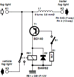
This is a simple Fog Lamp Switch Circuit Diagram. This circuit recommended to have a rear fog light on a trailer with the additional requirement that, when the trailer is coupled to the car, the rear fog light of the towing car has to be off. The circuit shown here is eminently suitable for this application. The circuit is placed near the rear fog light of the car. The 12-V connection to the lamp has to be interrupted and is instead connected to relay contacts 30 and 87A (K1, K3). When the rear fog light is turned on it will continue to operate normally.

 Fog Lamp Switch Circuit Diagram

Fog Lamp Switch Circuit Diagram


If a trailer with fog light is now connected to the trailer connector (7- or 13-way, K2), a current will flow through L1. L1 is a coil with about 8 turns, wound around reed contact S1. S1 will close because of the current through L1, which in turn energizes relay Re1 and the rear fog light of the car is switched off. The fog light of the trailer is on, obviously. The size of L1 depends on reed contact S1. The fog lamp is 21 W, so at 12 V there is a current of 1.75 A. L1 is sized for a current between 1.0 and 1.5 A, so that it is certain that the contact closes. The wire size has to be about 0.8 mm. The relay Re1 is an automotive relay that is capable of switching the lamp current. The voltage drop across L1 is negligible.  
 
Author : J. Geene Copyright :Elektor Electronics 2008
Continue reading...

Sunday, December 22, 2013

The price of cell phone jammer will be lower if you buy a large quantity

The runtime of the battery of cell phone jammer can reach 160 minutes.
Android cell phone bulk delete contacts. Sometimes we need to contact to delete, especially not deleted but by selectively delete contacts, are Android phones in only one by one manually delete? This is too much trouble, if many did not half an hour to complete can not. Are there any easy way? , Delete contacts, there are two ways, first is stated above on the cell phone one by one to delete, and another is to use the Gmail account will sync contacts to your cell phone Android cell phone bound, on the contrary Android cell phone on the contacts can also choose to sync to Gmail account contacts. The price of cell phone jammer will be lower if you buy a large quantity.
So we can use the second method for rapid bulk delete contacts operation. Here are the steps: Gmail mailbox into the bound on the Android cell phone on a PC, operating one of the contacts, delete contacts, removal is complete, and then on the cell phone contacts can be synchronized. Android cell phone WIFI connection but can not access. Some of the Android cell phone users will encounter this problem when the cell phone WIFI wireless network connection, you can connect to the wireless network, and the signal is very good, but the use of certain network support software (such as the Browser Shique or Market) is not working, there is a big delay. How is this going? cell phone jammer equips with the dedicated operation status indicator.
But problems may be due to the switching network standards, then the wireless router set to 802.11g, of course, 802.11b can, but at a slower pace. Since then, Internet WIFI connection but can not be satisfactorily resolved. Android cell phone to restore the factory settings. As a smartcell phone operating system Android is also built many other smartcell phone operating system features that are common, such as mobile phones are essential to restore the factory settings. Android cell phone how to set it correctly in order to restore the factory settings do? cell phone jammer has the high security requirement.
First of all, we must be clear that the restore factory settings this feature is not frequently used, because if the misuse of the consequences are very serious, and restore the factory settings can be understood literally, all the settings in the cell phone will be restored to factory condition.
Continue reading...

Friday, December 20, 2013

Build a Positive input Negative output Charge pump Circuit Diagram

How to Build a Positive input Negative output Charge pump Circuit Diagram. A simple means of generating a low-power voltage supply of opposite polarity from the main supply. Self oscillating driver produces pulses at a repetition frequency of 100 kHz. 

When the VMOS device is off, capacitor C is charged to the positive supply. When the VMOS transistor switches on, C delivers a negative voltage through the series diode to the output. The zener serves as a dissipative regulator.

Positive input Negative output Charge pump Circuit Diagram

 Positive input Negative output Charge pump Circuit Diagram

Continue reading...

Thursday, December 19, 2013

Measuring Milliohms with a Multimeter

Low values of resistance can be troublesome especially when large current s f low through them. A current of, say, 10 A passing through a terminal with a contact resistance of 50 m? will produce a voltage difference of 0.5 V. This resulting power loss of five watts is dissipated in the termination and can give rise to a dangerously high temperature which may degrade insulation around the wires.

Measuring Milliohms with a Multimeter Circuit Diagram

Measuring Milliohms with a Multimeter-Circuit Diagram

Measuring low values of resistance is not easy. Low cost multimeters do not include a milliohm measurement range and specialist equipment is expensive. The simple circuit described here allows milliohm measurements to be made safely on a standard ist equipment is expensive. The simple circuit described here allows milliohm measurements to be made safely on a standard multimeter. The circuit consists of little more than a 6 V voltage regulator and a mains adapter capable of supplying around 300 mA at 9 to 12 V.

The circuit supplies a fixed cur-rent output of 100 mA or 10 mA selected by switch S1. This connects either the 60 ? or 600 ? resistor into the constant current generator circuit. The resistor values are produced by paralleling two identical resistors; 120 ? and 1.2 k? from the E12 standard resistor range. Two test leads with probes are used to deliver current to the test resistance. The resultant voltage drop is measured by the multimeter (M1). With the test current set to100 mA a measurement of 1 mV indicates a resistance of 10 m?. At 10 mA (with S1 in the position shown in the diagram) a measurement of 1 mV indicates a resistance of 100 m? while 0.1 mV is equal to 1 m?. Diode D1 protects the meter from too high an input voltage.

With the voltmeter connected as shown in the diagram it measures not only the voltage drop across RX but also that produced by the resistance of the test leads, and probes. To make a true measurement, first touch the probes close together on the same lead of the test resistance and note the reading, now place the probes across the test resistance and note the reading again. The first reading measures just the test leads and probes while the second includes the resistance RX. Subtract the first measurement from the second to get the value of RX.

The accuracy of the measurements are influenced by the contact resistance of switch S1, the precision of resistors R1 to R4, the 6 V supply level and of course the accuracy of the measuring voltmeter. For optimum decoupling C1 should be fitted as close as possible to pin1 of IC1. An additional electrolytic capacitor of around 500 µF can be used at the input to the circuit if the input voltage from the AC power adapter exhibits excessive ripple.

Source:  http://www.ecircuitslab.com/2012/03/measuring-milliohms-with-multimeter.html
Continue reading...

Wednesday, December 18, 2013

A good business is not really the appreciation

 A good business is not really the appreciation of the work and marketing tool received suffering from markets and telephone product of the strength is the key to victory, of course, low comprehensive

listing of G808 last year continue to allow me to appreciate the dance of the Samsung. It is the process and result of performing every operational instruction of

cell phone jammer .
The replacement phone of HTC product cycle is very fast, almost did not take long on a machine Huang. HTC family of Windows machines Huang HTC HD3, do not know yet listed. While Android is in fact

the front is not long, nothing more than the G3, the Hero. I think for many people, especially Chinese people do not want to play the machine to send messages to call you taking pictures, do not

buy the HTC. If you have a business role, the entertainment capital of the class you want to see the movie, send email, browse the World Wide Web, play a large 3D games. Then you consider that HTC

well. The most important thing is that the HTC machine hardware configuration is very good, and that old-fashioned Nokia is completely different. To show the detailed status of

cell phone jammer .
I saw a little boy says: Im gay, I use the M8 - and then immediately replied: do not lose our gay face on the cnbeta. Now is not a phone as small as possible. You go to Europe and the United

States to take a look at those famous models, they go on the street holding his hands a large mobile phone to send text messages there. Looks super Fan children. - Suitable for girls with Sharp a

lot of heads are not small, is said to hand a small little girls no way to single-handedly control the Sharp. I phone is very large, two hands to get maintained, BlackBerry texting should at least

use two hands. - On the trend of mobile phones the size of argument, I am more biased in favor of mobile phone now or bigger only decent. The system administrator can screen cell phone jammer .
Millet mobile marketing strategies and models dismantling. Presentation online site finishing. Introduction: the popularity of millet phone and the millet mobile phone marketing strategy is

inseparable from millet phones with what kind of marketing strategy?
Continue reading...

Saturday, October 5, 2013

Up Down Timer For A Power Antenna

This up/down timer was designed to control a power antenna on a late-model vehicle. Normally, this vehicle uses a body computer to control the antenna. However, the person who owned the vehicle wanted to install his own high-powered audio stereo system. The original stereo system was tied in with the body computer and this meant that a separate antenna controller was required for the after-market sound system. Also, the power antenna fitted did not have limit switches inside, hence the need for a timed control circuit. Heres how the circuit works. first, assume that the radio antenna control output is not switched on - ie, the radio is switched off.

In that case, relay RLYC will be off and so relay RLYA will also be off, as is the motor. Conversely, when the radio is switched on, the radio antenna control output line switches to +12V. And when that happens, RLYC closes its contacts and applies power to the circuit. As a result, C2 (330OF) quickly charges via D4, while Q4 is biased on via D5 and R5. This ensures that Q3 and relay RLYB remain off. At the same time, Q2 is is turned on, thus turning on RLYA and applying power to the motor. This drives the antenna in the up direction. During this time, C1 charges via R2.

Up and down timer for a power antenna circuit schematic

When the voltage across the capacitor reaches +8.1V, Q1 turns on via ZD1 and so Q2 turns off and switches off the relay - ie, this gives the "up" timeout. Using the values shown for C1, R2 and ZD1 gives an "up" duration of approximately 6 seconds - long enough to fully extend the antenna. D1 discharges C1 (via resistor R1) when the +12V supply is later removed. When the radio is switched off (or a CD placed into the stereo unit), the radio antenna control output switches back to 0V. This does several things: first, it turns Q4 off and this allows Q3 to turn on due to the stored charge in C2. Q3 and RLYB now turn on for about six seconds - ie, while C2 discharges via R4 - and this switches power to the motor in the opposite direction to drive the antenna down. Diodes D4 and D5 are there to prevent C2 from discharging back via the circuitry around on Q1 and Q2.
Continue reading...

Wednesday, September 11, 2013

Making A Self Watering Plant with Arduino

Plants liven up any space by adding a sense of airiness and life. That is – of course – when you don’t forget to water them, and they shrivel up and die. I am very bad at remembering to water plants. That is why I built this self-watering plant to do it for me. Using a soil sensor, and an Arduino-controlled water pump, I have created a system that will never forget to do it.

Making A Self-Watering Plant with Arduino
 
Instead of remembering to water my plants when the soil goes dry, I only have to remember to once and a while refill the water reservoir. In this way, I have decreased my obligation to these plants and put it off to a much later date. Perhaps further iterations of this device can be connected to a rain barrel so that I won’t even have to worry about refilling my reservoir, and the entire system can be fully automated.
Continue reading...

Tuesday, September 10, 2013

A Li Ion Battery Charger with Load Sharing MCP73837

Batteries often serve as the main energy source for portable electronic devices. Although they depend on batteries, portable consumer electronic products, such as GPS devices and multi-media players, often consume energy directly from an ac-dc wall adapter or accessory power adapter (or “Auto Adapter”) when the battery is low or the device is in a stationary mode. Due to their cost effectiveness over their useful life, rechargeable batteries are often used for the power source of the portable electronic device.


Designing A Li-Ion Battery Charger with Load Sharing - MCP73837

 
Attributes such as “relatively high energy density” and “maintenance free” make Lithium-Ion (Li-Ion) batteries popular in the portable consumer electronic products. Refer to the application note, AN1088, “Selecting the Right Battery System For cost Sensitive Portable Applications While maintaining Excellent Quality” (DS01088) for characteristics of Li-Ion batteries. Some examples of how to properly design with Li-Ion batteries will be discussed in this application note.
Continue reading...

Testing the Photovoltaic Effect with a Transistor

Most photovoltaic cells are made of silicon chip above which there resides a very thin layer of noble metal through which around 1% of photon particles enter the material and activates electron flow. Here I’m showing how to make one simple solar panel using transistor.

Testing the Photovoltaic Effect with a Transistor
Continue reading...

Tuesday, September 3, 2013

A Short Wave Regenerative Receiver

Sensitivity and selectivity are the major concerns of a short wave enthusiast when he looks up for a receiver. Commercial communications models with superhet circuitry surely satisfy his requirements, but these are expensive. He would rather go for a homebrewed radio, being a regenerative receiver an affordable choice.

Im also a short wave listener and for some time I used my familys MW and SW tube radio, Philips brand. Then I switched to a Sony ICF-7600 with ceramic filters in the IF stages. High selectivity was attained with this radio receiver.

A Short Wave Regenerative Receiver Circuit Diagram

 I then discovered how much fun it was to build radios in my spare time, having tested a variety of designs available in books and on the web. Finally, I managed to make my own designs. One of them is shown in Fig. 1. It is a nice performer and will tune from the 22 meter international broadcasting band down to the 11 meter band.

It is best that the 100 pF variable capacitor be a vernier type. Tuning will be easier this way.

Q1 is the amplifier-detector and along with its associated circuitry forms a common collector Colpitts oscillator that not actually oscillates: it operates as a regenerative amplifier, with R9 as the reaction control. In achieving this result, the transistors input capacitance plays an important role. The oscillating mode is employed when copying CW or SSB. Otherwise, the stage should be left very near the threshold of oscillation for maximum sensitivity and selectivity.

Q2 and Q3 form a high gain audio amplifier and ample volume should be expected at the output. This is why a volume control has been included in the circuit. A high impedance crystal earphone should be used at the output.

Pictures of My Prototype:


Below a sheet of metal used as a ground system:


Ing. Ramón Vargas Patrón rvargas@inictel.gob.pe
Continue reading...