Thursday, September 18, 2014
USB Switch Schematic Wiring diagram Schematic

Saturday, September 13, 2014
New Automatic Load Sensing Power Switch
New Automatic Load Sensing Power Switch Circuit Diagram
Parts |
| C1, C3 | 2 | 10uF 35V Electrolytic Capacitor | |
| C2 | 1 | 1uF 35V Electrolytic Capacitor | |
| R1 | 1 | 0.1 Ohm 10W Resistor | |
| R2 | 1 | 27K 1/2W Resistor | |
| R3, R4 | 1 | 1K 1/4W Resistor | |
| R5 | 1 | 470K 1/4W Resistor | |
| R6 | 1 | 4.7K 1/2W Resistor | |
| R7 | 1 | 10K 1/4W Resistor | |
| D1, D2, D4 | 3 | 1N4004 Rectifier Diode | |
| D3 | 1 | 1N4744 15V 1 Watt Zener Diode | |
| U1 | 1 | LM358N Dual Op Amp IC | |
| Q1 | 1 | 2N3904 NPN Transistor | |
| K1 | 1 | Relay, 12VDC Coil, 120VAC 10A Contacts | |
| S1 | 1 | SPST Switch 120AVC, 10A | |
| MISC | 1 | Board, Wire, Socket For U1, Case, Mains Plug, Socket |
- This schema is designed for 120V operation. For 240V operation, resistors R2 and R6 will need to be changed.
- A maximum of 5A can be used as the master unless the wattage of R1 is increased S1 provides a manual bypass switch.
- THis schema is not isolated from the mains supply. Because of this, you must exercise extreme caution when working around the schema if it is plugged in.
Friday, June 6, 2014
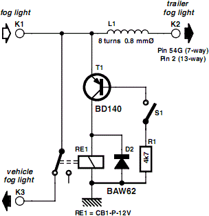
Build a Fog Lamp Switch Circuit Diagram
Fog Lamp Switch Circuit Diagram
Thursday, October 10, 2013
Clap Switch Circuit Diagram

Wednesday, October 9, 2013
Cheap Switch Mode DC DC Converter

Tuesday, October 8, 2013
Computer Off Switch
How often does it happen that you close down Windows and then forget to turn off the computer? This circuit does that automatically. After Windows is shut down there is a ‘click’ a second later and the PC is disconnected from the mains. Surprisingly enough, this switch fits in some older computer cases. If the circuit doesn’t fit then it will have to be housed in a separate enclosure. That is why a supply voltage of 5 V was selected. This voltage can be obtained from a USB port when the circuit has to be on the outside of the PC case. It is best to solder the mains wires straight onto the switch and to insulate them with heat shrink sleeving. C8 is charged via D1. This is how the power supply voltage for IC1 is obtained. A square wave oscillator is built around IC1a, R1 and C9, which drives inverters IC1c to f.
The frequency is about 50 kHz. The four inverters in parallel power the voltage multiplier, which has a multiplication of 3, and is built from C1 to C3 and D2 to D5. This is used to charge C5 to C7 to a voltage of about 9 V. The generated voltage is clearly lower than the theoretical 3x4.8=14.4 V, because some voltage is lost across the PN-junctions of the diodes. C5 to C7 form the buffer that powers the coil of the switch when switching off. The capacitors charge up in about two seconds after switching on. The circuit is now ready for use. When Windows is closed down, the 5-V power supply voltage disappears. C4 is discharged via R2 and this results in a ‘0’ at the input of inverter IC1b. The output then becomes a ‘1’, which causes T1 to turn on.
Circuit diagram:

Computer Off Switch Circuit Diagram
A voltage is now applied to the coil in the mains switch and the power supply of the PC is turned off. T1 is a type BSS295 because the resistance of the coil is only 24R. When the PC is switched on, the circuit draws a peak current of about 200 mA, after which the current consumption drops to about 300 µA. The current when switching on could be higher because this is strongly dependent on the characteristics of the 5-V power supply and the supply rails in the PC. There isn’t much to say about the construction of the circuit itself. The only things to take care with are the mains wires to the switch. The mains voltage may not appear at the connections to the coil. That is why there has to be a distance of at least 6 mm between the conductors that are connected to the mains and the conductors that are connected to the low-voltage part of the circuit.
Author: Uwe Kardel - Copyright: Elektor Electronics Magazine
Source : www.extremecircuits.net
Thursday, October 3, 2013
Switch Timer For Bathroom Light

Monday, September 30, 2013
Speaker Headphone Switch Circuit Diagram For Computers

ATX Power Switch Substitute
 If the motherboard documentation is poor, you should verify the earth pin using a continuity tester. The resistor is only needed if you want to be able to switch on the PC within ten seconds after switching it off. It discharges the capacitor quickly enough to make this possible. With a 1-kΩ resistor, the time constant is around 0.5 s. Since the capacitor also tends to stabilize the voltage, this circuit could also help in situations in which the ATX power supply switches off unintentionally due to voltage fluctuations on the PWR Supply On line.
Sunday, September 29, 2013
RC Remote Control Switch
Picture of the project:

The servo signal, which consists of pulses from 1 to 2 ms duration, depending on the desired position, enters the circuit via pin 1 of connector K1. Two buffers from IC2 provide the necessary buffering after which the signal is differentiated by C2. This has the effect that at each rising edge a negative start signal is presented to pin 2 of IC1. D1 and R4 make sure that at the falling edge the voltage at pin 2 of IC2 does not become too high. IC1 (TLC555) is an old faithful in a CMOS version.
A standard version (such as the NE555) works just as well, but this IC draws an unnecessarily high current, while we strive to keep the current consumption as low as possible in the model. The aforementioned 555 is configured as a one-shot. The pulse-duration depends on the combination of R2/C1. Lowering the voltage on pin 5 also affects the time. This results in reducing the length of the pulse. In this circuit the pulse at the output of IC will last just over 1.5 ms when T1 does not conduct.
Circuit diagram:

When T1 does conduct, the duration will be a little shorter than 1.5 ms. We will explain the purpose of this a little later on. Via IC2.C, the fixed-length pulse is, presented to the clock input of a D-flip-flop. As a consequence, the flip-flip will remember the state of the input (servo signal). The result is that when the servo-pulse is longer than the pulse form the 555, output Q will be high, otherwise the output will be low. It is possible, in practice, that the servo signal is nearly the same length as the output from the 555.
A small amount of variation in the servo signal could therefore easily cause the output to ‘chatter’, that is, the output could be high at one time and low the next. To prevent this chatter there is feedback in the form of R1, R3 and T1. This circuit makes sure that when the flip-flip has decided that the servo-pulse is longer than the 555’s pulse (and signals this by making output Q high), the pulse duration from the 555 is made a little shorter. The length of the servo-signal will now have to be reduced by a reasonable amount before the servo-pulse becomes shorter than the 555’s pulse.
Parts and PCB layout:

The moment this happens, T1 will stop conducting and the mono-stable time will become a little longer. The servo-pulse will now have to be longer by a reasonable amount before the flip-flip changes back again. This principle is called hysteresis. Jumper JP1 lets you choose between the normal or inverted output signals. Buffers IC2.D through to IC2.F together with R5 drive output transistor T2, which in turn drives the output. Note that the load may draw a maximum current of 100 mA. Diode D2 has been added so that inductive loads can be switched as well (for example, electrically operated pneu-matic valves).
COMPONENTS LIST
Resistors:
R1 = 470k
R2 = 150k
R3 = 47k
R4 = 100k
R5 = 4k7
Capacitors:
C1 = 10nF
C2 = 1nF
C3,C4 = 100nF
Semiconductors:
D1 = BAT85 or similar Schottky diode
D2 = 1N4148
IC1 = CMOS 555 (e.g., TLC555 or ICM7555)
IC2 = 4049
IC3 = 4013
T1,T2 = BC547B
Miscellaneous:
JP1 = jumper with 3-way pinheader
K1 = servo cable
K2 = 2-way pinheader or 2 solder pins
Saturday, September 28, 2013
USB Switch For Printers Circuit Diagram

Sunday, September 22, 2013
Smart Foot Switch Circuit
Such jobs as jewel cutting and polishing require the workers to switch on/ off two electrical appliances one after another repeatedly for two different services on the same workpiece. This is cumbersome as they need to fully concentrate on delicate handwork on precious jewels. Switching in such situations cannot be done by hand, and doing it by foot using ordinary switches is too tedious. This is mainly because of the difficulty in sensing and controlling the switch position by foot. Ordinary pushbutton switches make or break a contact momentarily, and they cannot hold the keypress status. You need a bistable multivibrator with two independent trigger inputs to solve this problem.
Here’s a smart foot switch based on dual negative-edge triggered master slave JK flip-flop IC 74LS76 (IC1). J1 and J2 inputs are conneted to 5V through resistors R2 and R5 (each 10k), respectively.K1 and K2 inputs are grounded. Preset pins 2 and 7 are shorted and connected to 5V via resistor R7 (10k). Push-to-on switch S3 connected to the preset inputs is also grounded. Clock and clear inputs of the two flip-flops are cross-connected, i.e. CLK1 (pin 1) is conneted to CLR2 (pin 8) and CLR1 (pin 3) is connected to CLK2 ( pin 6). Clock input pins 1 and 6 are pulled up high through resistors R1 and R4 (each 4.7k), respectively.
Circuit Diagram:
 Smrat tFoot Switch Circuit diagram
Push-to-on switches S1 and S2 are connected between clock and ground of the flip-flops. Switch S1 activates device 1, while switch S2 activates device 2. Switch S3 activates both device 1 and device 2 simultaneously. Device status is indicated by LED1 and LED2. Glowing of LED1 and LED2 indicates that device 1 and device 2, respectively, are in on condition. The LEDs are connected from +5V to Q1 (pin 14) and Q2 (pin 10) of IC1 through resistors R3 and R6, respectively.
Initially when the power supply is switched on, Q1 and Q2 outputs of the JK flip-flops are at low level (logic 0). When switch S1 is pressed for the first time, the high level (logic 1) present at J1 input is transferred to Q1 output on the trailing edge of clock (CLK1). The high level (logic 1) at Q1 activates relay RL1 through pin 16 of IC ULN2003 (IC2), turning on device 1 via its normally-opened (N/O) contacts. Clock CLK1 of flip-flop IC1(A) is also connected to clear input CLR2 of flip-flop IC1(B) so as to clear it asynchronously. Switch debounces don’t affect the circuit as the same J1 state is being transferred to Q1 output on succeeding trailing edges. At the same time, device 2 is switched off.
When switch S2 is pressed, flip-flop IC1(A) gets cleared via CLR1 and the high state of J2 input of flip-flop IC1(B) is transferred to its Q2 output on the trailing edge of clock (CLK2). This high level (logic1) activates relay RL2 through pin 15 of IC2, turning on device 2 via its N/O contacts. At the same time, device 1 is switched off.
Now if you want to turn on both the devices simultaniously, press switch S3 momentarily. Switch S3 provides ground to preset inputs PRE1 and PRE2 of flipflops IC1(A) and IC1(B), making their Q1 and Q2 outputs high, which energises both the relays turning on the two devices. LEDs glow to indicate that both the devices are ‘on.’
Place all the three switches (S1 through S3) where you can easily press them by foot when required. The LEDs can also be mounted at a convenient location to know whether the devices are turned on.
Author : JAYAN A.R. Copyright : Electronics For You Mach 2004
Wednesday, September 4, 2013
Parking Light Switch
Parking Light Switch Circuit Diagram

Notes:
This is a very simple light switching circuit using a single transistor and relay to control an external mains powered light. Relay RLA is drawn with two changeover contacts, but a relay with two make contacts can also be used. The contacts MUST be rated at 240V AC and at least 3 Amp (or higher) to safely switch loads of up to 500 Watts. Once energized the relay latches through contacts RLA1 and the external lamp is switched via contact RLA2.
Setting Up:
Wait until darkness and shine your vehicles headlights at the ORP12 Photocell. Adjust the 100k potentiometer until the relay triggers. Turn off the headlights and press S2 to turn off the relay. The external light should go off. It may be necessary to place a plastic tube of about 1 inch in length so that only light emitted by a cars headlights reaches the photocell. This will prevent unwanted triggering.
The light can also be manually controlled by pressing S1 which will latch the circuit, and S2 will turn off the lamp again.
Tuesday, September 3, 2013
Schematic 10 Way Electronic Switch
10 Way Electronic Switch Circuit Diagram

The schematic is shown above, and two switches S1 and S2 are used to control the outputs. The main work is done by U2 a CMOS4017 decade counter divider IC. At switch on, C1 is quickly charged by R4 and a brief reset pulse is applied to to the reset pins of both U1 and U2. This results in U1, a 7 segment display display driver and decade counter showing "zero" on the 7 segment display and pin 3 (which is the output zero) of the 4017 becoming high.
Each time S1 is pressed the clock input of U2 is incremented, by one count and the display and 4017 will cycle through all 10 outputs. A separate reset switch is not provided as the display reads the currently selected output.
When the 4017 is on a particular output, for example zero, then the controlled circuit can be turned on or off using switch S2. To latch the output a type JK flip-flop is used at each of the ten outputs. This works as follows. When the 4017 is at output zero, pin 3 will be high. This enables both JK inputs of the flip flop (U4A at output zero) and the circuit can then be toggled via pulses applied from switch S2. The Q output of each flip-flop drives and NPN transistor and then a small relay. The NPN transistors can be any general purpose type, e.g. 2N2222, BC108, BC548 etc. The relay allows external loads of different voltage and current to this circuit to be controlled.
For clarity, the schematic is drawn with outputs, zero, six and nine shown only. The pinouts for the CMOS ICs 4017 and 4026 can be found in the practical section.
The CMOS 4026 is available at ESR Electronics in the UK.
If required, the external circuits power supply can be used to power the driver transistor and relay. This is shown on output 6, the dotted lines representing the power coming from an external battery. The only other requirement here is that the external circuits common negative terminal is tied to this circuits common chassis (negative) terminal.
Monday, September 2, 2013
Sound Operated Switch
Sound Operated Switch Circuit diagram

It should be noted that this circuit does not "latch". The relay and LED operate momentarily in response to audio peaks.
Thursday, December 20, 2012
Photo Albums Wiring Diagrams Gang Switch

Option 3 Fixture Between Two Three Way Switches Power Through Switch.

Av And Automation Industry Emagazine Which One Should I Use Part.

Way Switch Wiring Diagram Power Enters At Light Fixture Box.

Photo Albums Wiring Diagrams Three Gang Two Way Switch.

Option 6 Power To Light To Light To Switch To Switch.

Way Switch Wiring Yelp.

How To Replace A 3 Way Switch Kanderson Enterprises.

Normal Three Way Switches You Have Two Wiring Boxes Where The Switches.

Leviton 3 Way Switch Wiring Diagram Leviton Decora Speed Control.

Is Basically A 3 Way Circuit With A 4 Way Switch Added Between The 2.