Showing posts with label diagram. Show all posts
Showing posts with label diagram. Show all posts
Sunday, November 2, 2014
AUTOMATIC AIRFLOW DETECTOR ELECTRONIC DIAGRAM
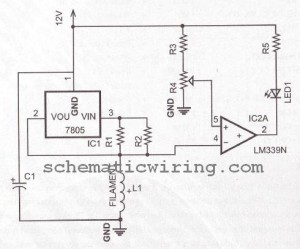
AUTOMATIC AIRFLOW DETECTOR ELECTRONIC DIAGRAM
Sensor used in this circuit is a bulb filament. If there is no airflow, the filament resistance would give low value. On the other hand, if there is airflow, the filament resistance would varies. The variation of the resistance is caused by the heat difference between filament. It also effects to the voltage variation passing through that filament. That voltage difference will be processed by LM339 op-amp and displayed by the LED.
Parts list :
- LED1 : LED 5mm
- IC1 volt regulator : LM7805
- Polar Capacitor C1 : 47 uF/15V
- Resistor R1 : 100 ohm
- Resistor R2 : 470 ohm
- Resistor R3 : 10k ohm
- Potensiometer R4 : 100k ohm
- Resistor R5 : 1k ohm
- IC2 op-amp : LM339
- Bulb filament
- Power supply/battery 12V

Thursday, October 16, 2014
Build a Bass Treble Tone Control Circuit Diagram
How build a Bass-Treble Tone Control Circuit Diagram . The LM1036 is a DC controlled tone (bass/treble), volume and balance circuit for stereo applications in car radio, TV and audio systems. An additional control input allows loudness compensation to be simply effected. Four control inputs provide control of the bass, treble, balance and volume functions through application of DC voltages from a remote control system or, alternatively, from four potentiometers which may be biased from a zener regulated supply provided on the circuit. Each tone response is defined by a single capacitor chosen to give the desired characteristic.
Build a Bass-Treble Tone Control Circuit Diagram

Features:
- Wide supply voltage range, 9V to 16V
- Large volume control range, 75 dB typical
- Tone control, ±15 dB typical
- Channel separation, 75 dB typical
- Low distortion, 0.06% typical for an input level of 0.3 Vrms
- High signal to noise, 80 dB typical for an input level of 0.3 Vrms
- Few external components required
Vcc can be anything between 9V to 16V and the output capacitors are
10uF/25V electrolytic.
Wednesday, September 24, 2014
Generating Stepped Voltage Circuit Diagram
This circuit converts an enter sign into one that may be composed of a number of discrete steps but which re- mains in a different way identical to the enter sign, because the steps are of equivalent peak, the harmonic con- tent of the output sign shall be dependent upon the amplitude of the enter sign.
This characteristic is very useful within the making of electronic tune.
 The circuit uses quantitised pulse-width modulation for the including of the step-formed enters sign. Pulse-width modulation is acquired by comparing a triangular voltage with the analogue enter sign by the use of a comparator; the quantitising, that may be the including of the steps, takes place by replacing the triangular voltage with a stepped voltage. The transistor transfers the rate on C2 to capacitor C4.
Throughout the following part cycle C2 is rerated by means of Dl. ln this manner the voltage across C4 increases in discrete steps, the height of the steps being deter- mined by the ratio C2:4. Whilst the voltage across C4 rises above a certain price, N2 switches transistor T2 on by means of gate N3 and disrates capacitor C4. Whilst the capacitor is completely disrated, N2 switches off T2 and C4 continues to rate again in discrete steps. The stepped voltage uses to the inverting enter of lC2 which is l hooked up as a comparator. Low- move clear out R4/C7 within the output of lC2 converts the heartbeat-width modulated sign again to an analogue one. The d.c. voltage degree at the non- inverting enter uses by potentiometer P2 to part the significance of the stepped voltage. The environment of P1 depends on the enter sign which should be attenuated such that the maximum price at the slider of Pl is at all times smaller than i the utmost price of the stepped I voltage. The collection of steps can also be decided on by various the worth of C4. lt is imaginable to use a varicap in preference to C4 with the varicap voltage being managed by the tune program or the enter sign. Attention grabbing and person results can also be acquired on this method.
This characteristic is very useful within the making of electronic tune.
Throughout the following part cycle C2 is rerated by means of Dl. ln this manner the voltage across C4 increases in discrete steps, the height of the steps being deter- mined by the ratio C2:4. Whilst the voltage across C4 rises above a certain price, N2 switches transistor T2 on by means of gate N3 and disrates capacitor C4. Whilst the capacitor is completely disrated, N2 switches off T2 and C4 continues to rate again in discrete steps. The stepped voltage uses to the inverting enter of lC2 which is l hooked up as a comparator. Low- move clear out R4/C7 within the output of lC2 converts the heartbeat-width modulated sign again to an analogue one. The d.c. voltage degree at the non- inverting enter uses by potentiometer P2 to part the significance of the stepped voltage. The environment of P1 depends on the enter sign which should be attenuated such that the maximum price at the slider of Pl is at all times smaller than i the utmost price of the stepped I voltage. The collection of steps can also be decided on by various the worth of C4. lt is imaginable to use a varicap in preference to C4 with the varicap voltage being managed by the tune program or the enter sign. Attention grabbing and person results can also be acquired on this method.
Monday, September 22, 2014
Fuse Box Toyota 1990 4runner Relay Diagram
Fuse Box Toyota 1990 4runner Relay Diagram - Here are new post for Fuse Box Toyota 1990 4runner Relay Diagram.


Fuse Panel Layout Diagram Parts: charge, hazzard horn, dome light, headlight, alternator, headlight control relay, EFI relay, EFI relay, CMH relay.
Continue reading...
Fuse Box Toyota 1990 4runner Relay Diagram


Fuse Panel Layout Diagram Parts: charge, hazzard horn, dome light, headlight, alternator, headlight control relay, EFI relay, EFI relay, CMH relay.
Sunday, September 21, 2014
Fuse Box BMW 745 V8 2003 Diagram
Fuse Box BMW 745 V8 2003 Diagram - Here are new post for Fuse Box BMW 745 V8 2003 Diagram.
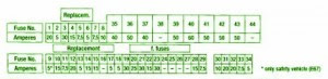

Fuse Panel Layout Diagram Parts: Radio, rear screen, roller sun blind, seat adjustment, seat heating, servotronic, speed control, starter diesel engine, steering column adjustment, CD changer, central locking system, LK doors, central locking system, remote control, cigar lighter, transmission control, instrument cluster, lighting, multi function steering, wheel, on board monitor, parking brake, airbag, air conditioner, anti roll stabilizer, auxiliary heater diesel, blower, wiper/washer systemdiagnosis plug, burning heater, deflation warning system, door window lift, damper control, engine control gasoline, heated steering wheel, ignition starter switch, independent heater, adaptive head light, ABS.
Continue reading...
Fuse Box BMW 745 V8 2003 Diagram
Fuse Panel Layout Diagram Parts: Radio, rear screen, roller sun blind, seat adjustment, seat heating, servotronic, speed control, starter diesel engine, steering column adjustment, CD changer, central locking system, LK doors, central locking system, remote control, cigar lighter, transmission control, instrument cluster, lighting, multi function steering, wheel, on board monitor, parking brake, airbag, air conditioner, anti roll stabilizer, auxiliary heater diesel, blower, wiper/washer systemdiagnosis plug, burning heater, deflation warning system, door window lift, damper control, engine control gasoline, heated steering wheel, ignition starter switch, independent heater, adaptive head light, ABS.
Thursday, September 18, 2014
USB Switch Schematic Wiring diagram Schematic
Anyone experimenting or developing USB ported peripheral hardware soon be comes irritated by the need to disconnect and connect the plug in order to reestablish communication with the PC. This process is necessary for example each time the peripheral equipment is reset or a new version of the firmware is installed. As well as tiresome it eventually leads to excessive contact wear in the USB connector. The answer is to build this electronic isolator which disconnects the peripheral device at the touch of a button. This is guaranteed to reduce any physical wear and tear and restore calm once again to the workplace.
USB Switch Schematic Circuit Image
The schema uses a quad analogue switch type 74HC4066. Two of the switches in the package are used to isolate the data path. The remaining two are used in a classic bistable flip-flop configuration which is normally built using transistors. A power MOSFET switches the power supply current to the USB device. Capacitor C2 ensures that the flip flop always powers-up in a defined state when plugged into the USB socket (‘B’ in the diagram).
The peripheral device connected to USB socket ‘A’ will therefore always be ‘not connected’ until pushbutton S2 is pressed. This flips the bistable, turning on both analogue gates in the data lines and switching the MOSFET on. The PC now recognises the USB device. Pressing S1 disconnects the device.
Circuit diagram :USB Switch Schematic Circuit Diagram
The schema does not sequence the connections as a physical USB connector does; the power supply connection strips are slightly longer than the two inner data carrying strips to ensure the peripheral receives power before the data signals are connected. The electronic switch does not suffer from the same contact problems as the physical connector so these measures are not required in the schema. The simple schema can quite easily be constructed on a small square of perforated strip-board.
The design uses the 74HC(T)4066 type analogue switch, these have better characteristics compared to the standard 4066 device. The USB switch is suitable for both low-speed (1.5 MBit/ s) and full-speed (12 MBit/s) USB ports applications but the proper ties of the analogue switches and perf-board construction will not support hi-speed (480 MBit/s) USB operation.
The IRFD9024 MOSFET can pass a current of up to 500 mA to the peripheral device with-out any problem.
http://streampowers.blogspot.com/2012/07/touch-switchs.html
Fuse Box Toyota 1997 Camry CE Diagram
Fuse Box Toyota 1997 Camry CE Diagram - Here are new post for Fuse Box Toyota 1997 Camry CE Diagram.


Fuse Panel Layout Diagram Parts: engine main relay, horn relay, RDI fuse, CDS fuse, headlamp, head relay, St relay, main fuse-high current, EFI relay.
Continue reading...
Fuse Box Toyota 1997 Camry CE Diagram


Fuse Panel Layout Diagram Parts: engine main relay, horn relay, RDI fuse, CDS fuse, headlamp, head relay, St relay, main fuse-high current, EFI relay.
Sunday, September 14, 2014
Mercedes Explanation Fuse Box Year 230 Diagram
Fuse Box Mercedes 230 Diagram - Below is Fuse Box Mercedes 230 Diagram.


Fuse Panel Layout Diagram Parts: electronic accelerator, first gear start relay, combination relay, power seat diode, exterior lamp, failure monitoring unit, convenience relay, seat belt warning relay, power seat relay, auxiliary fan relay, preresistor, headlamp washer relay, air injection relay, power window relay, parking brake.
Continue reading...
Fuse Box Mercedes 230 Diagram
Fuse Panel Layout Diagram Parts: electronic accelerator, first gear start relay, combination relay, power seat diode, exterior lamp, failure monitoring unit, convenience relay, seat belt warning relay, power seat relay, auxiliary fan relay, preresistor, headlamp washer relay, air injection relay, power window relay, parking brake.
Friday, September 5, 2014
Digital H V AC Switcher Wiring diagram Schematic
This is a digital H-V or high voltage AC switcher schema diagram, Switching a high voltage AC requires use of opto couplers to isolate the High Voltage from the micro controller. A basic schema to trigger an SCR is shown in Fig. 67 -lA. This schema has the disadvantage that the blocking voltage of the photon-coupler output device determines the schema-blocking voltage, irrespective of higher main SCR capability. Adding capacitor Cl to the schema, as shown in Fig. 67-lB, will reduce the dV!dt seen by the photoncoupler output device.
Digital H-V AC Switcher Circuit Diagram

Digital H-V AC Switcher Circuit Diagram
Click right and Save image and zoom for best view
The energy stored in Cl, when discharged into the gate of SCRl, will improve the dildt capability of the main SCR. Using a separate power supply for the coupler adds flexibility to the trigger schema; it removes the limitation of the blocking voltage capability of the photon-coupler output device. The flexibility adds cost and more than one power supply might be necessary for multiple SCRs if no common reference points are available. 67-lC, Rl can be connected to Point A. which will remove the voltage from the coupler after SCRl is triggered. `or to Point B so that the coupler output will always be biased by input voltage.
The former is preferred since it decreases the power dissipation in Rl. A more practical form of SCR triggering is shown in Fig. 67 -IF. Trigger energy is obtained from the anode su]Jply and stored in Cl. Coupler voltage is limited by the zener voltage. This approach permits switching of higher voltages than the blocking voltage capability of the output device of the photon coupler. To reduce the power losses in Rl and to obtain shorter time constants for charging Cl, the zener diode is used instead of a resistor. A guide for selecting the component values would consist of the following steps: Choose Cl in a range of 0.05 to 1 p.F.
The maximum value might be limited by the recharging time constant (RL + R1) C1 while the minimum value will be set by the minimum pulse width required to ensure SCR latching. R2 is determined from peak gate current limits, if applicable, and minimum pulse width requirements. Select a zener diode. A 25-V zener is a practical value, since this will meet the usual gate requirement of 20 V and 20 0. This diode will also eliminate spurious triggering because of voltage transients. Photon coupler triggering is ideal for the SCR`s driving inductive loads. By ensuring that the LASCR latches on, it can supply gate current to SCRl until it stays on.
The former is preferred since it decreases the power dissipation in Rl. A more practical form of SCR triggering is shown in Fig. 67 -IF. Trigger energy is obtained from the anode su]Jply and stored in Cl. Coupler voltage is limited by the zener voltage. This approach permits switching of higher voltages than the blocking voltage capability of the output device of the photon coupler. To reduce the power losses in Rl and to obtain shorter time constants for charging Cl, the zener diode is used instead of a resistor. A guide for selecting the component values would consist of the following steps: Choose Cl in a range of 0.05 to 1 p.F.
The maximum value might be limited by the recharging time constant (RL + R1) C1 while the minimum value will be set by the minimum pulse width required to ensure SCR latching. R2 is determined from peak gate current limits, if applicable, and minimum pulse width requirements. Select a zener diode. A 25-V zener is a practical value, since this will meet the usual gate requirement of 20 V and 20 0. This diode will also eliminate spurious triggering because of voltage transients. Photon coupler triggering is ideal for the SCR`s driving inductive loads. By ensuring that the LASCR latches on, it can supply gate current to SCRl until it stays on.
Wednesday, September 3, 2014
1998 Ford f800 Wiring Diagram
 |
| 1998 Ford f800 Wiring Diagram |
(More Detail Visit Here)
This is 1998 Ford f800 Wiring Diagram: power distribution, indicator, air switch, switch closed, diesel, switch testing, buzzer module, engine alarm, stihes.
Saturday, August 30, 2014
Soldering Station Weller 40 Watts Circuits Wiring diagram
This is a Soldering Station Weller 40 Watts Circuits Diagram, WLC100 model, she is one of the simplest, however very efficient, ideal for those who want to build a small soldering station. The Weller WLC100 as the main component is a triac which controls the voltage that goes to the resistor, thus making the iron to vary the temperature. He is a very robust Soldering station has a power ranging from 5-40 watts uses the tips (SPG40) and resistance (HE40), ideal for hobbyists, students, and hobbyists.
Soldering Station Weller 40 Watts Circuits Diagram
List of components
R1 = 15 Ohms, 1/8 Watt 5%
P1 = 250K pot
C1 = 823K, 250V
D1, D2 = 1N4004 D3 = Diac, bilateral trigger type Triac
Q1 = 400V/25A, Q4012LPH * (Teccor) or BTA08600c (Philips), or equivalent
ATTENTION: The Triac has an isolated tab, so if you need to replace sure to use the same type.

Friday, August 29, 2014
1998 Chevrolet Suburban 1500 Wirng Diagram
 |
| 1998 Chevrolet Suburban 1500 Wirng Diagram |
(More Detail Visit Here)
This is 1998 Chevrolet Suburban 1500 Wirng Diagram: headlight, beam, derect, horn, conv centr, switch, marker, battery, blu fuse, neutral switch, dimmer, ignition coil, module, air actuator, coolant sensor, pump connector, thotile, oxigen, map, windshield, alternator.
Thursday, August 28, 2014
Dual White Noise and Pink Noise Generator Wiring diagram Schematic
This is a generator schema which is very useful, it simultaneously generates two types of noise, pink and white. The noise generator is a schema that produces electrical noise. Noise generators are used to test, measure noise, frequency response, and other parameters. The schema described here is based on the operational amplifier 741.
Dual White Noise and Pink Noise Generator Circuit Diagram
Friday, June 6, 2014
Active Crossover Circuit Diagram with TL074
Simple Active Crossover Circuit Diagram with TL074. An audio source, like a mixer, preamp, EQ, or a recorder, is fed to the input of the Electronic Crossover Circuit. This signal is either AC or coupling, depending on the setting of switch 51, the non-inverting input of buffer amplifier Ul-a, a section of a quad BIFET, low amp TL074 noise made by Texas Instruments op.
This stage has a gain of 2, and its output is distributed to both a low pass filter made by R4, R5, C2, C3, and Uld op-amp, and a high-pass filter made by R6, R7, C4, C5, and op amp ULC. These are12 dB / octave Butter worth filters. The response of the Butter worth filter was chosen because it gives the best compromise between the damping and phase.
Active Crossover Circuit Diagram with TL074

The values of capacitors and resistors varies depending on the selected connection that your device works. The filter outputs are fed to a balancing network made by R8, R9, RIO, R14 and potentiometer RLL balance. When the potentiometer is at its center position, there is a unity gain bandwidths for both high and low filters. Power for the electronic circuit is regulated by Crossover R12, RI3, Dl and D2, and decoupled by C6 and C7.
Sorced By : Circuitsstream
Simple Vlf Converter Circuit Diagram
This is The Simple Vlf Converter Circuit Diagram. This converter uses a low-pass filter instead of the usual tuned circuit so the only tuning required is with the receiver. The dual-gate MOSFET and FET used in the mixer and oscillator aren`t critical.
Simple Vlf Converter Circuit Diagram
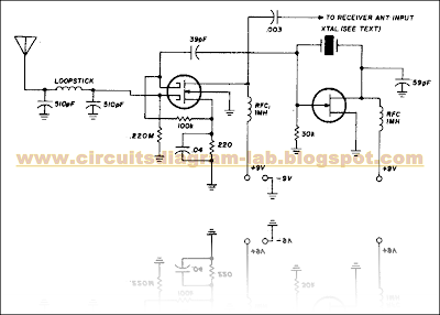
Any crystal having a frequency compatible with the receiver tuning range may be used. For example, with a 3500 kHz crystal, 3500 kHz on the receiver dial corresponds to zero kHz; 3600 to 100 kHz; 3700 to 200 kHz, etc (At 3500 khz on the receiver all one can hear is the converter oscillator, and VLF signals start to come in about 20 kHz higher).
Build a Fog Lamp Switch Circuit Diagram
This is a simple Fog Lamp Switch Circuit Diagram. This circuit recommended to have a rear fog light on a trailer with the additional requirement that, when the trailer is coupled to the car, the rear fog light of the towing car has to be off. The circuit shown here is eminently suitable for this application. The circuit is placed near the rear fog light of the car. The 12-V connection to the lamp has to be interrupted and is instead connected to relay contacts 30 and 87A (K1, K3). When the rear fog light is turned on it will continue to operate normally.
Fog Lamp Switch Circuit Diagram
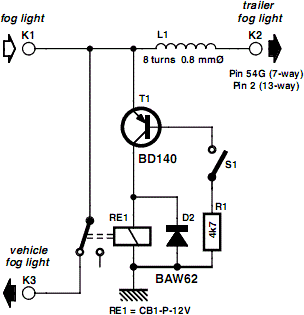
If a trailer with fog light is now connected to the trailer connector (7- or 13-way, K2), a current will flow through L1. L1 is a coil with about 8 turns, wound around reed contact S1. S1 will close because of the current through L1, which in turn energizes relay Re1 and the rear fog light of the car is switched off. The fog light of the trailer is on, obviously. The size of L1 depends on reed contact S1. The fog lamp is 21 W, so at 12 V there is a current of 1.75 A. L1 is sized for a current between 1.0 and 1.5 A, so that it is certain that the contact closes. The wire size has to be about 0.8 mm. The relay Re1 is an automotive relay that is capable of switching the lamp current. The voltage drop across L1 is negligible.
Author : J. Geene Copyright :Elektor Electronics 2008
1 5V Battery to 5V Voltage Converter Circuit Diagram
This is a Simple 1.5V Battery to 5V Voltage Converter Circuit Diagram. Stable and secure 5V DC (at 200mA max) from an ordinary 1.5V AA sized cell. At the heart of this circuit is IC1 MAX756 from Maxim, which is a CMOS step-up DC-DC switching regulator for small, low input voltage or battery-powered systems.
Simple 1.5V Battery to 5V Voltage Converter Circuit Diagram

MAX756 accepts a positive input voltage down to 0.7V and converts it to a higher pin selectable output voltage of 5V (or 3.3V). Typical full-load efficiency for the this IC is greater than 87%. Max756 combine a switch-mode regulator with an N-channel MOSFET, precision voltage reference, and power-fail detector in a single monolithic device. The MOSFET is a “sense-FET” type for best efficiency, and has a very low gate threshold voltage to ensure start-up under low-battery voltage conditions (1.1V typ).
The circuit can be easily wired on a very small rectangular common PCB.All connections should be kept as short as possible. If available,try to add a good quality 8 pin DIP socket for IC1. Note that the power inductor’s (L1) DC resistance significantly affects efficiency. For highest efficiency, limit L1’s DC resistance to 0.03 Ohm or less. A thru-hole type standard power inductor can be used. Similarly, the ESR of all capacitors (bypass and filter) affects circuit efficiency. Best performance is obtained by using specialized low-ESR capacitors.
Simple F and V Converter Circuit Diagram
This is a best Frequency/Voltage Converter circuit diagram proportional voltage by the use of a frequency-to-voltage (F/V) converter. Teledyne Semiconductor`s Type TSC9402 is a versatile IC. Not only can it convert voltage into frequency, but also frequency into voltage. It is thus eminently suitable for use in an add-on unit for measuring frequencies with a multimeter.
Best F and V Converter Circuit Diagram

Only a few additional components are required for this.. Just one calibration point sets the center of the measuring range (or of that part of the range that is used most frequently). The frequency-proportional direct voltage at the output (pin 12—amp out) contains interference pulses at levels up to 0.7 V. If these have an adverse effect on the multimeter, they can be suppressed with the aid of a simple RC network.
The output voltage, U0, is calculated by: tfo=C/rei(Ci + 12 pF) R2fm Because the internal capacitance often has a greater value than the 12 pF taken here, the formula does not yield an absolute value. The circuit has a frequency range of dc to 10 kHz. At 10 kHz, the formula gives a value of 3.4 V. The circuit draws a current of not more than 1 mA.
Sourced By : Circuitsstream
Beacon Transmitter Circuit Diagram
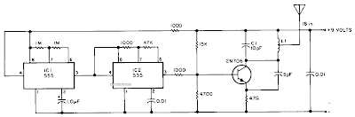
Simple Beacon Transmitter Circuit Diagram.This transmitter can be used for transmitter hunts, for remote key finding, or for radio telemetry in model rockets. It can be tuned to the two meter band or other VHF bands by charging Cl and Ll. 11 is four turns of #20 enameled wire air wound, 0.25 inch in diameter (use a drill bit), 0.2 inch long, center tapped. The antenna can be 18 inches of any type of wire. IC2 functions as an audio oscillator that is turned on and off by IC1 about once per second. The range of the transmitter is several hundred yards.
Simple Beacon Transmitter Circuit Diagram
2MHz Square Wave Generator Circuit Diagram
2MHz Square Wave Generator Circuit Diagram. With the values shown the circuit generates a 2-MHz symmetrical square wave. Changing capacitors Cl and C2 to 0.01 µ¥ results in a frequency of 500 Hz. For the particular integrated circuits and power supply voltages (5.0 V), the reliable operating range of Rl = R2 is 2 k ohm to 4 k ohm.
2MHz Square Wave Generator Circuit Diagram

Subscribe to:
Posts (Atom)