Thursday, November 20, 2014
Metronome Generator Circuit using NE555
Notes.
- The circuit can be wired on a general purpose PCB or common board.
- The circuit can be powered from a 9V PP3 battery.
- The POT R1 can be used to adjust the rhythm of the sound.
- The POT R2 can be used as volume control.
- The speaker k1 can be a n 8 Ohm tweeter.

Wednesday, November 19, 2014
Audio Peak Indicator Circuit
The main function of a series of Audio Peak indicator is to determine the occurrence of the peak level of audio signal that is more than +4 dB, equivalent to 1.25 V rms. If the received audio signal Audio Peak Indicator more than +4 dB was the LEDs in series Peak Audio This indicator will light. Audio Peak indicator circuit is mounted on the output audio system.

R1 = 10Kohm
R2 = 1.2Kohm
R3 = 220Kohm
R4-5 = 4.7Kohm
C1 = 47uF 25V
C2 = 2.2uF 25V
Q1-2 = BC550C
D1 = LED RED
Tuesday, November 18, 2014
6 Watt Audio Amplifier Schematic Circuit with TDA1519
The audio amplifier circuit is on the TDA1519 amplifier IC that is based in audio applications, which is not a aerial achievement ability can be used. The ambit TDA1519 is a ability of 2×6 watts.
The TDA1519 is an amplifier congenital Class B dual-output advance in a 9-by-line (SIL) artificial amalgamation boilerplate achievement is primarily developed for car radio applications.
Key Features of the audio amplifier IC TDA1519 are: Requires few alien components, anchored gain, acceptable bounce drive, aphasiac / standby mode, thermal protection, about-face polarity safe. Tda1519 amplifier ability rating, 14.4 volts.
Thursday, November 13, 2014
BC557 based Flashing Eyes circuit with explanation
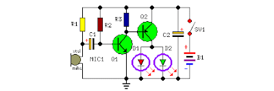 Two-LED-eyes follow the rhythm of music or speech, 3V Battery-operated device suitable for pins or badges
This circuit was purposely designed as a funny Halloween gadget. It should be placed to the rear of a badge or pin bearing a typical Halloween character image, e.g. a pumpkin, skull, black cat, witch, ghost etc. Two LEDs are fixed in place of the eyes of the character and will shine more or less brightly following the rhythm of the music or speech picked-up from surroundings by a small microphone. Two transistors provide the necessary amplification and drive the LEDs.
Parts:
R1 = 10K
R2 = 1M
R3 = 1K
C1 = 4.7uF-25V
C2 = 47uF-25V
D1 = 2mm LED
D2 = 2mm LED
Q1 = BC547
Q2 = BC557
B1 = 3V Battery
SW1 = SPST Switch
MIC1 = Electret Mic
Notes:
* Any general purpose, small signal transistor can be used for Q1 and Q2, but please note that R3 could require adjustment, depending on the gain of Q1. For medium gain transistors, the suggested value should do the job. High gain transistors will require a lower value for R3, i.e. about 390 – 470 Ohm. You can substitute R3 with a 1K Trimmer in order to set precisely the threshold of the circuit.
* Any LED type and color can be used, but small, 2mm diameter, high efficiency LEDs will produce a better effect.
* No limiting resistors are required for D1 and D2 even if this could seem incorrect.
* Stand-by current consumption of the circuit is about 1.5mA.
* Depending on dimensions of your badge, you can choose from a wide variety of battery types:
* 2 x 1.5 V batteries type: AA, AAA, AAAA, button clock-type, photo-camera type & others.
* 2 x 1.4 V mercury batteries, button clock-type.
Friday, October 31, 2014
230V Flasher Circuit
 |
230V Flasher Circuit diagram |
# Be careful when you deal with 230V
# Build this circuit on a PCB
# Use only mentioned values.
Wednesday, October 29, 2014
Electronic Motor Starter Diagram Circuit
 Switch S1 is used to turn on the pump, while switch S2 is used to turn off the pump. While making over-/under-voltage setting, disconnect C2 temporarily. Capacitor C2 prevents relay chattering due to rapid voltage fluctuations. Regulator IC 7809 gives the 9V regulated supply to soft switch as well as the relay after filtering by capacitor C4. A suitable miniature circuit breaker is used for automatic over-current protection. Green LED (LED1) indicates that the motor is ‘on’ and red LED (LED2) indicates that the power is ‘on’. The motor is connected to the normally-open contact of the relay. When the relay energizes, the motor turns on.
Monday, October 27, 2014
STK4038 bassed 60 watt audio amplifier circuit project and explanation
Using the STK4038X audio amplifier IC, can be designed a very simple high power and efficiency audio power amplifier . This circuit is manufactured by Sanyo Corporation and will provide a output power of 60 watts on a 8 ohms load or 4 ohms load with 0.008% distortion .
The output power that is provided by this audio IC , can be more higher , but with more distortion.
If you will use a 8 ohms load you must power this audio amplifier project from a dual +/- 40 volts DC power supply and if you’ll use a 4 ohms load you must power this audio project form a dual +/- 33.5 volts DC power source.
To prevent over heating the STK4038X audio power IC must be heatsinked on a good heatsink .
Also you must use a very well filtered power supply ( a 10000uF capacitor will be fine for this audio project) .
Saturday, October 25, 2014
Circuit Mobile Phone Battery Charger

Thursday, October 23, 2014
Power Supply Variable 1 3V 12 2V 1A Circuit

Description:
R2 to set the output voltage. The maximum current is determined by R3, over-current protection circuit inside the LM723 to detect the voltage on R3, if it reaches 0.65 V, the voltage output will be off her. So the current through R3 can not exceed 0.65 / R3 although output short-circuit in his.
C3 and C4 are ceramic capacitors, as much as possible directly soldered to the PCB, this is because the LM723 is prone to oscillation that is not cool.
LM723 works with 9.5V input voltage to 40 V DC and the LM723 can generate its own current of 150mA when the output voltage is not more than 6-7V under input voltage.
Specifications:
Output (value estimated):
Vmin = (R4 + R5) / (R5 * 1.3)
Vmax = (7.15 / R5) * (R4 + R5)
Imax = 0.65/R3
Max. Power on R3: 0.42/R3
Min. DC Input Voltage (pin 12 to pin 7): Vmax + 5
Component List:
B1 40V/2.5A
C1 2200uF (3300uF even better)
C2 4.7uF
C3 100nF
C4 1NF
C5 330nF
C6 100uF
Green LED D1
D2 1N4003
F1 0.2A F
F2 2A M
IC1 LM723 (in a DIL14 plastic package)
R1 1k
R2 Pot. 5k
R3 0.56R/2W
R4 3.3k
R5 4.7k
S1 250V/1A
T1 2N3055 on a heatsink 5K / W
TR1 220V/17V/1.5
Thursday, October 16, 2014
Build a Bass Treble Tone Control Circuit Diagram

- Wide supply voltage range, 9V to 16V
- Large volume control range, 75 dB typical
- Tone control, ±15 dB typical
- Channel separation, 75 dB typical
- Low distortion, 0.06% typical for an input level of 0.3 Vrms
- High signal to noise, 80 dB typical for an input level of 0.3 Vrms
- Few external components required
Vcc can be anything between 9V to 16V and the output capacitors are
10uF/25V electrolytic.
Sunday, October 5, 2014
PIC16F628 Digital Clock Timer circuit and explanation
This clock timer uses a PIC16F628 microcontroller to display 3 and 1/2 digit time and control an external load. It can be programmed to time from 1 to 59 minutes. The clock includes a calendar with leap year and optional daylight savings adjustments. The timer output can be set from 1 to 59 minutes and manually switched on and off. The clock also has a correction feature that allows an additional second to be added every so many hours to compensate for a slightly slow running oscillator. The oscillator uses a common 32.768 KHz watch crystal and the frequency can be adjusted slightly with the 24pF capacitor on the right side of the crystal.
Wednesday, October 1, 2014
Simple Fish Caller Circuit
Varying the two potentiometers produces a wide variety of sounds. You may be lucky and hit on one that will bring in the big ones. An inexpensive waterproof housing is thick walled polythene bag with a few lead sinkers inside. An on-off toggle switch can be manipulated without opening the bag when switching power on and off. The bag opening is sealed with good quality electrical tape to make system waterproof. Tape seal should be renewed after each use.

Wednesday, September 24, 2014
Generating Stepped Voltage Circuit Diagram
This characteristic is very useful within the making of electronic tune.

Throughout the following part cycle C2 is rerated by means of Dl. ln this manner the voltage across C4 increases in discrete steps, the height of the steps being deter- mined by the ratio C2:4. Whilst the voltage across C4 rises above a certain price, N2 switches transistor T2 on by means of gate N3 and disrates capacitor C4. Whilst the capacitor is completely disrated, N2 switches off T2 and C4 continues to rate again in discrete steps. The stepped voltage uses to the inverting enter of lC2 which is l hooked up as a comparator. Low- move clear out R4/C7 within the output of lC2 converts the heartbeat-width modulated sign again to an analogue one. The d.c. voltage degree at the non- inverting enter uses by potentiometer P2 to part the significance of the stepped voltage. The environment of P1 depends on the enter sign which should be attenuated such that the maximum price at the slider of Pl is at all times smaller than i the utmost price of the stepped I voltage. The collection of steps can also be decided on by various the worth of C4. lt is imaginable to use a varicap in preference to C4 with the varicap voltage being managed by the tune program or the enter sign. Attention grabbing and person results can also be acquired on this method.
Tuesday, September 23, 2014
Portable Guitar Amplifier Circuit

Portable Guitar Amplifier Circuit Parts:
R1______________22K 1/4W Resistor
C1______________10µF 25V Electrolytic Capacitor
C2_____________100nF 63V Polyester or Ceramic Capacitor
C3_____________220µF 25V Electrolytic Capacitor
IC1__________TDA7052 Audio power amplifier IC
J1,J2__________6.3mm Stereo Jack sockets (switched)
SPKR___________8 Ohm Loudspeaker (See Notes)
B1________________9V PP3 Battery or
3V Battery (2 x 1.5V AA, AAA Cells in series etc.)
Clip for PP3 Battery or socket for 2 x 1.5V AA or AAA Cells
Portable Guitar Amplifier Technical data:
Max output power: 1.5W @ 9V supply - 8 Ohm load; 60mW @ 3V supply - 8 Ohm load
Frequency response: Flat from 20Hz to 20kHz
Total harmonic distortion @ 100mW output: 0.2%
Max input voltage @ 3V supply: 8mV RMS
Minimum input voltage for Fuzz-box operation: 18mV RMS @ 3V supply
Current consumption @ 400mW and 9V supply: 200mA
Current consumption @ 250mW and 9V supply: 150mA
Current consumption @ 60mW and 3V supply: 80mA
Quiescent current consumption: 6mA @ 9V, 4mA @ 3V supply
Fuzz-box current consumption: 3mA @ 3V supply
Thursday, September 18, 2014
USB Switch Schematic Wiring diagram Schematic
Friday, September 12, 2014
Simple accu charger circuit
Wednesday, September 10, 2014
555 Timer for DC to DC Converter Circuit
| 555 Timer for DC to DC Converter |
Monday, September 8, 2014
LM12 High Power Amplifier circuit
| Schematic High Power amplifier with LM12 |
Friday, September 5, 2014
Digital H V AC Switcher Wiring diagram Schematic
Digital H-V AC Switcher Circuit Diagram

The former is preferred since it decreases the power dissipation in Rl. A more practical form of SCR triggering is shown in Fig. 67 -IF. Trigger energy is obtained from the anode su]Jply and stored in Cl. Coupler voltage is limited by the zener voltage. This approach permits switching of higher voltages than the blocking voltage capability of the output device of the photon coupler. To reduce the power losses in Rl and to obtain shorter time constants for charging Cl, the zener diode is used instead of a resistor. A guide for selecting the component values would consist of the following steps: Choose Cl in a range of 0.05 to 1 p.F.
The maximum value might be limited by the recharging time constant (RL + R1) C1 while the minimum value will be set by the minimum pulse width required to ensure SCR latching. R2 is determined from peak gate current limits, if applicable, and minimum pulse width requirements. Select a zener diode. A 25-V zener is a practical value, since this will meet the usual gate requirement of 20 V and 20 0. This diode will also eliminate spurious triggering because of voltage transients. Photon coupler triggering is ideal for the SCR`s driving inductive loads. By ensuring that the LASCR latches on, it can supply gate current to SCRl until it stays on.
Tuesday, September 2, 2014
Simple Inverter circuit with IC556 timer chip
This circuit is low power inverter , in this circuit only save a few components, about 9 parts. Voltage input from 10 volt to 16 volt DC into 60-Hz. And then voltage will be raised to about 115 V with power 25 W. The first section of IC 556 timer chip is wire as an astable oscilator with R2 and C1 setting the frequncy. The output is available at IC 556 pin 5. The second section is wired as a phase inverter. That output is available at IC 556 pin 9.
Schematic low inverter below :
