Wednesday, November 12, 2014
Build Power Amplifier LM3876 Simply and Powerfull Power Amplifier
The chip on which the amplifier is based, a Type LM3876, is a member of the Overture family from National Semiconductor, All members of this family are pin-compatible and mutually interchangeable. They are typified by an internal protection (called SPIKE). In practice, the diftection ference between them is the power output. The series was described on the basis of the LM3886 in an earlier issue*.
The PCB has been designed so what it can accommodate the LM3876 (50W) as well as the LM3886 (150W). Because of this, pin5 of the IC on the board is connected to the positive supply line. This connection is not needed for the LM3876, since its pin5 is not (internally) connected (NC).
The IC is located at the side of the board to facilitate fitting it to a heat sink as shown in the photograph.
An important aspect for optimum performance is the decoupling of the unregulated supply lines by C 7-10. All earth connections go to a single terminal on the board.
Air-cored inductor L1 consists of 13 turns of 1mm dia. enamelled copper wire with an inner diameter of 10mm. The completed inductor is pushed over R7 and its terminals soldered to those of the resistor.
All electrolytic capacitors must be mounted upright. The amplifier can be muted with a single-pole switch connected to the MUTE input (pin8). This function is enabled when the switch is open. If muting is not required, solder a wire bridge across the mute terminals on the board.
Boucherot network R6-C6 is not normally required in this application, but provision has been made for it for use in other applications.
According to the manufacturers, both chips are optimalized for a load of 8 Ohm. The output power is lower when a 4 Ohm load is used or when the supply voltage is reduced. When a 4 Ohm load is used, the SPIKE protection becomes active when the supply voltage is about 27V, resulting a in a reduction of the power output to 10W. This means that it is not advisable to use loudspeaker with an impedance <8 ohm.
For best result you can expand power amplifier using BPA-200 Amplifier
Part listResistor:
R1, R3 = 1 k
R2, R4, R5 = 18k
R6 = see text
R7 = 10R, 5 Watt
R8, R9 = 22k
Capacitors:
C1 = 2.2 uF
C2 = 220 uF, 160 V
C3 = 22 uF, 40 V
C4 = 47 pF
C5 = 100 uF, 40 V
C6 = see text
C7, C8 = 100 nF
C9, C10 = 1000 uF, 40 V
Inductors:
L1 = 0.7 uH - see text
Integrated circuits:
IC1 = LM3876T
Miscellaneous:
Heat sink for IC1 <1.5 k w-1
Single-pole switch - see text


Thursday, November 6, 2014
Power Supply Failure Alarm
Thursday, October 23, 2014
Power Supply Variable 1 3V 12 2V 1A Circuit

Description:
R2 to set the output voltage. The maximum current is determined by R3, over-current protection circuit inside the LM723 to detect the voltage on R3, if it reaches 0.65 V, the voltage output will be off her. So the current through R3 can not exceed 0.65 / R3 although output short-circuit in his.
C3 and C4 are ceramic capacitors, as much as possible directly soldered to the PCB, this is because the LM723 is prone to oscillation that is not cool.
LM723 works with 9.5V input voltage to 40 V DC and the LM723 can generate its own current of 150mA when the output voltage is not more than 6-7V under input voltage.
Specifications:
Output (value estimated):
Vmin = (R4 + R5) / (R5 * 1.3)
Vmax = (7.15 / R5) * (R4 + R5)
Imax = 0.65/R3
Max. Power on R3: 0.42/R3
Min. DC Input Voltage (pin 12 to pin 7): Vmax + 5
Component List:
B1 40V/2.5A
C1 2200uF (3300uF even better)
C2 4.7uF
C3 100nF
C4 1NF
C5 330nF
C6 100uF
Green LED D1
D2 1N4003
F1 0.2A F
F2 2A M
IC1 LM723 (in a DIL14 plastic package)
R1 1k
R2 Pot. 5k
R3 0.56R/2W
R4 3.3k
R5 4.7k
S1 250V/1A
T1 2N3055 on a heatsink 5K / W
TR1 220V/17V/1.5
Friday, October 10, 2014
Power Amplifier OCL 50W by 741 2N3055 MJ2955 with PCB
This is old circuit Power amp OCL, But easy circuit and very nice. To use for play music in your home. It low cost too. It use IC 741 or LF351(good) and Transistor x 4 (2N3055+MJ2955+BD139+BD140) and little component. Power supply volt +35V/-35V and 3A for Mono, 5A for Stereo.

Circuit Power Amp OCL by 741+2N3055+MJ2955

Thursday, September 18, 2014
High Power Amplifier 300W


PCB

SPECIFICATIONS | |
POWER OUTPUT | 200W rms/8 ohm |
310W rms/4 ohm | |
800W rms/8 ohm (Bridge mode) | |
FREQUENCE RESPONSE | 20HZ-20KHZ +/-0.5dB |
INPUT SENSITIVITY | 1V for 200W/300W |
HUM AND NOISE | -105dB |
THD | <0.1% |
DAMPING FACTOR | 65 |
Saturday, September 13, 2014
New Automatic Load Sensing Power Switch
New Automatic Load Sensing Power Switch Circuit Diagram
Parts |
| C1, C3 | 2 | 10uF 35V Electrolytic Capacitor | |
| C2 | 1 | 1uF 35V Electrolytic Capacitor | |
| R1 | 1 | 0.1 Ohm 10W Resistor | |
| R2 | 1 | 27K 1/2W Resistor | |
| R3, R4 | 1 | 1K 1/4W Resistor | |
| R5 | 1 | 470K 1/4W Resistor | |
| R6 | 1 | 4.7K 1/2W Resistor | |
| R7 | 1 | 10K 1/4W Resistor | |
| D1, D2, D4 | 3 | 1N4004 Rectifier Diode | |
| D3 | 1 | 1N4744 15V 1 Watt Zener Diode | |
| U1 | 1 | LM358N Dual Op Amp IC | |
| Q1 | 1 | 2N3904 NPN Transistor | |
| K1 | 1 | Relay, 12VDC Coil, 120VAC 10A Contacts | |
| S1 | 1 | SPST Switch 120AVC, 10A | |
| MISC | 1 | Board, Wire, Socket For U1, Case, Mains Plug, Socket |
- This schema is designed for 120V operation. For 240V operation, resistors R2 and R6 will need to be changed.
- A maximum of 5A can be used as the master unless the wattage of R1 is increased S1 provides a manual bypass switch.
- THis schema is not isolated from the mains supply. Because of this, you must exercise extreme caution when working around the schema if it is plugged in.
Monday, September 8, 2014
LM12 High Power Amplifier circuit
| Schematic High Power amplifier with LM12 |
Sunday, September 7, 2014
6 18 Volt audio power amplifier
C1 = 1uF
C2 = 220uF
C3 = 100uF
C4 = 47uF
C5 = 1000uF
C6 = 100nF
C7 = 470pF
C10 = 47pF
Sunday, August 31, 2014
5 Volt power Supply

This is 5 volt power supply schema diagram.This schema regulates 5V.Input voltage is 6V to 12V.

Parts
# LM7805
# 100nF condensators
# 100uF condensator
# 10uF condensator
# N4002 diode
# LED
# 470 Ohm resistor
Saturday, December 21, 2013
Simple 0 50V 2A Bench Power Supply Circuit Diagram

Vlose p1=100uA*Rp1
This lose voltage regulate output voltage rate of output current is compare between reference voltage of P3 and lose voltage on R11.T3 is protecting short circuit with R11. For reduce out put voltage to 0v should parallel one resistor 470 ohm in out put. Minimum voltage is 0.4v. The maximum output voltage is fixed with R1b and should not become over of 50v. Therefore your transformer should give 36V, 3A with 4700uF capacitor. T6, T5, T7 need heatsilk.

R1b = read the text
R2 = 10 K
R3, R7 = 3.3 k
R4 = 390 Ohm
R5 = 47 K
R6 = 3.3 K 1Watt
R8 = 180 Ohm
R9, R10 = 0.47 Ohm 3Watt
R11 = 0.075 Ohm 2Watt
R12 = 470 Ohm
P1 = 500K liner potentiometer
P2 = 4.7 K potentiometer
P3 = 10 K potentiometer
C1 = 1nF
C2 = 10nF
C3 = 22nF
C4 = 47mF 63v electrolytic
C5 = 4700mF 80v electrolytic
T1, T2 = BC161
T3, T4 = BD141
T5 = BD241
T6, T7 = 2V3055
D1, D2 = 1N4148
D3, D4 = 1N4001
IC1, IC2 = LM10C
Friday, December 20, 2013
Medium Power Inverter Circuit Diagram

Thursday, December 19, 2013
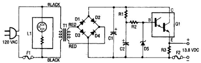
13 8Vdc 2A Regulated Power Supply Circuit Diagram
Tuesday, December 17, 2013
Soft Start For Switching Power Supply
When the supply cannot cope with this, it fails or the fuse blows. It is, therefore, advisable to disable the regulator at switch-on (via the on/off input). until the relevant capacitor has been charged. When the regulator then starts to draw current, the charging current has already dropped to a level which does not overload the voltage source.
Circuit diagram:

The circuit in the diagram provides an output voltage of 5 V and is supplied by a 24 V source. The regulator need not be disabled until the capacitor is fully charged: when the potential across the capacitor has reached a level of half or more of the input voltage, all is well. This is why the zener diode in the diagram is rated at 15 V. Many regulators produced by National Semiconductor have an integral on/off switch, and this is used in the present circuit.
The input is intended for TTL signals, and usually consists of a transistor whose base is accessible externally. This means that a higher switching voltage may be applied via a series resistor: the value of this in the present circuit is 22 kΩ. When the voltage across the capacitor reaches a level of about 17 V, transistor T1 comes on, whereupon the regulator is enabled.
Saturday, October 5, 2013
Up Down Timer For A Power Antenna
In that case, relay RLYC will be off and so relay RLYA will also be off, as is the motor. Conversely, when the radio is switched on, the radio antenna control output line switches to +12V. And when that happens, RLYC closes its contacts and applies power to the circuit. As a result, C2 (330OF) quickly charges via D4, while Q4 is biased on via D5 and R5. This ensures that Q3 and relay RLYB remain off. At the same time, Q2 is is turned on, thus turning on RLYA and applying power to the motor. This drives the antenna in the up direction. During this time, C1 charges via R2.

When the voltage across the capacitor reaches +8.1V, Q1 turns on via ZD1 and so Q2 turns off and switches off the relay - ie, this gives the "up" timeout. Using the values shown for C1, R2 and ZD1 gives an "up" duration of approximately 6 seconds - long enough to fully extend the antenna. D1 discharges C1 (via resistor R1) when the +12V supply is later removed. When the radio is switched off (or a CD placed into the stereo unit), the radio antenna control output switches back to 0V. This does several things: first, it turns Q4 off and this allows Q3 to turn on due to the stored charge in C2. Q3 and RLYB now turn on for about six seconds - ie, while C2 discharges via R4 - and this switches power to the motor in the opposite direction to drive the antenna down. Diodes D4 and D5 are there to prevent C2 from discharging back via the circuitry around on Q1 and Q2.
Thursday, October 3, 2013
Computer Power Supply for Battery Charger
Some workbenches can’t help ending up looking like a rats nest of cables and equipment, so its always an advantage if a piece of mains equipment can be removed from somewhere to free up an extra mains socket. Here we are using the ubiquitous PC as a battery charger. An unused serial interface port can supply enough current to charge (or trickle charge) low-capacity Nickel Cadmium (NiCd) batteries. You could for example, use the batteries in a radio and charge them during use.

The three serial port connections TxD, DTR, and RTS, when not in use, are at –10 V and can supply a current of around 10 to 20mA (they are short-circuit protected). The circuit shown supplies a charging current of approximately 30mA. If it is necessary to alter the polarity of the charging circuit then it is a simple job to reverse the diodes and using software, switch the port signals +10 V. Those interested could also write a software routine to automatically recharge the batteries.
Source : www.extremecircuits.net
Monday, September 30, 2013
ATX Power Switch Substitute
 If the motherboard documentation is poor, you should verify the earth pin using a continuity tester. The resistor is only needed if you want to be able to switch on the PC within ten seconds after switching it off. It discharges the capacitor quickly enough to make this possible. With a 1-kΩ resistor, the time constant is around 0.5 s. Since the capacitor also tends to stabilize the voltage, this circuit could also help in situations in which the ATX power supply switches off unintentionally due to voltage fluctuations on the PWR Supply On line.
Friday, September 27, 2013
Variable DC Power Supply Circuit Diagram
Voltage Range: 0.7V to 24V, Current Range: 50mA to 2A
A variable dc power supply is one of the most useful tools on the electronics hobbyists workbench. This circuit is not an absolute novelty, but it is simple, reliable, "rugged" and short-proof, featuring variable voltage up to 24V and variable current limiting up to 2A. You can adapt it to your own requirements as explained in the notes below.
Circuit Diagram :

Variable DC Power Supply Circuit Diagram
Parts:
P1 = 500R
P2 = 10K
R1 = 2.2K-1/2w
R2 = 2.2K-1/2w
R3 = 330R
R4 = 150R
R5 = 1R-5W
C1 = 35V-3300uF
D1 = 1N5402
D2 = 1N5402
D3 = 5mm Red Led
C2 = 63V-1uF
Q1 = BC182
Q2 = BD139
Q3 = BC212
Q4 = 2N3055
SW1 = SPST Mains Switch
T1 = 36VCT-Transformer
Notes:
- P1 sets the maximum output current you want to be delivered by the power supply at a given output voltage.
- P2 sets the output voltage and must be a logarithmic taper type, in order to obtain a more linear scale voltage indication.
- You can choose the Transformer on the grounds of maximum voltage and current output needed. Best choices are: 36, 40 or 48V center-tapped and 50, 75, 80 or 100VA.
- Capacitor C1 can be 2200 to 6800µF, 35 to 50V.
- Q4 must be mounted on a good heatsink in order to withstand sustained output short-circuit. In some cases the rear panel of the metal box in which you will enclose the circuit can do the job.
- The 2N3055 transistor (Q4) can be replaced with TIP3055 type.
Source : www.redcircuits.com
Monday, September 23, 2013
Very Low Dropout Adjustable Breadboard Power Supply
 MIC2941 regulator has guaranteed 1.25A output
Low dropout, only 40mV - 400mV compared to 1.25V - 2.0V for LM317. This means you can use a wider range of output voltages including generating 3.3V from as low as 3.7V (such as 3 AAs or a lithium ion battery)!
Short circuit and overheating protection
Input diode to protect circuitry from negative voltages or AC power supplies.
2.1mm DC jack and terminal connector for voltage inputs
Two indicator LEDs for high and low voltages
Output selection switch to select from 3.3v, 5v and Adjustable
On-board potentiometer for adjusting voltage from 1.25V up to within 0.5V of the input voltage. (20V max)
On/Off switch for entire board

Saturday, September 21, 2013
High Power Headphone Amplifier Using BD139 40
- Reverb drive amplifier - ideal for low and medium impedance reverb tanks
- High current line driver - suitable for very long balanced lines
- Low power speaker amplifier - better performance than small integrated amps
- ... and of course, a headphone amp.
As a headphone amplifier, this design is very similar to others on the ESP site, but the main difference is that this one (and P70) has been built and fully tested. The design is fairly standard, and every variation was checked out before arriving at the final circuit. A photo of the prototype is shown below, and at only 64 x 38mm (2.5 x 1.5 inches) it is very small - naturally, the heatsink is not included in the dimensions.
The amplifier is capable of delivering around 1.5W into 8 ohm headphones, and 2.2W into 32 ohms - this is vastly more than will ever be needed in practice. The use of a 120 Ohm output resistor is recommended, as this is supposed to be the standard source impedance for headphones. Unfortunately, many users have found that their phones perform better when driven from a low impedance source.
 Prototype Headphone Amplifier
The circuit is based on an opamp, with its output current boosted by a pair of transistors. Distortion is well below my measurement threshold at all levels below clipping into any impedance. Noise is virtually non-existent - even with a compression driver held to my ear, I could barely hear any, and I couldnt hear any with headphones.
WARNING
Headphones are rated in dB SPL at 1mW, and this amplifier (like many other similar headphone amps) is capable of producing extreme SPLs. The levels obtainable are sufficient to cause almost instantaneous permanent hearing damage! Never operate the amp at very high levels, and never switch the amplifier on with signal while wearing you headphones.
Always start with the volume control at minimum, and gradually increase the level until it is comfortable, but not too loud. Because of the very low distortion, it is easy to increase the level too far without noticing. Your ears are precious - safeguard them at all times.
Note the warning above - this is serious. Most headphones are capable of at least 94dB SPL at 1 mW, with some as high as 107dB SPL. Even 10mW is enough to create sound levels capable of causing hearing damage, so you must be very careful to avoid damaging levels.
| Continuous dB SPL | Maximum Exposure Time |
| 85 | 8 hours |
| 88 | 4 hours |
| 91 | 2 hours |
| 94 | 1 hour |
| 97 | 30 minutes |
| 100 | 15 minutes |
| 103 | 7.5 minutes |
| 106 | < 4 minutes |
| 109 | < 2minutes |
| 112 | ~ 1 minute |
| 115 | ~ 30 seconds |
Note that the exposure time is for any 24 hour period, and is halved for each 3dB SPL above 85dB. The above shows the accepted standards for recommended permissible exposure time for continuous time weighted average noise, according to NIOSH (National Institute for Occupational Safety and Health) and CDC (Centers for Disease Control). Although these standards are US based, they apply pretty much equally in most countries - hearing loss does not respect national boundaries.
Description
The amplifier itself is fairly conventional, and is very similar to another shown on this site (see Project 24). This amplifier does not include the active volume control, because in general it is far easier to get a good log pot (or simply fake the pots law as described in Project 01). Likewise, it does not include the cross-feed described in Project 109. If this is desired, it is very easy to implement on a small piece of tag board, or even sky hook the few components off the bypass switch. Full details of how to do this will be included in the construction guide when PCBs are available.
The output transistors are biased using only resistors, rather than constant current sources. Extensive testing showed that using current sources made no discernible difference to performance, but increased the complexity and PCB size. Using separate caps for each biasing diode does make a difference though - and although it is relatively minor, the use of the two caps is justified IMHO.
The bias diodes should be 1N4148 or similar - power diodes are not recommended, as their forward voltage is too low. This may result in distortion around the crossover region, where one transistor turns off and the other on. As shown, crossover distortion is absolutely unmeasurable with the equipment I have available.
 Figure 1 - Headphone Amplifier Circuit Diagram
Above is the schematic of one channel. Resistors and caps use the suffix R for the right channel. The second half of the dual opamp powers the right channel. Note that the volume control shown is optional, and is not on the PCB. If needed, it may be mounted in a convenient location and the output connected to the inputs of the board as shown. D1 and D2 (L and R) are 1N4148 or similar.
One of the reasons the amp is so quiet is that the entire board runs from a regulated supply, so hum (in particular) is eliminated. Although an unregulated supply can be used, this is not recommended. The supply should be separate from that used for your preamp, because of the relatively high current drawn by the amplifier (at least with low impedance phones). A P05 preamp supply can be used, and will ensure optimum performance.
The prototype amplifier has flat frequency response from 10Hz to over 100kHz. Distortion is below my measurement threshold with any level or load impedance, and output impedance is almost immeasurably low. Your headphones may be designed to operate from a 120Ω source impedance (many are), so this may be added if it improves sound quality. Adding any series resistance will reduce the available power, but it is already far greater than you can use. Without series resistance, the minimum power into various load impedances is given below (based on ±15V supplies).
| Impedance | Power (Direct) | 120 Ohm Feed |
| 8 Ohms | 1.5 W | 35 mW |
| 32 Ohms | 2.2 W | 99 mW |
| 65 Ohms | 1.1 W | 136 mW |
| 120 Ohms | 595 mW | 149 mW |
| 300 Ohms | 238 mW | 121 mW |
| 600 Ohms | 119 mW | 82 mW |
Construction
While it may be possible to build it using Veroboard or similar, there is a high risk that it will oscillate because of the very wide bandwidth of the amplifier. A capacitor may be added in parallel with R4 (L and R) to reduce the bandwidth if stability problems are encountered. Although I used an NE5532 opamp for the prototype, the circuit will also work with a TL072, but at reduced power. You may also substitute an OPA2134 or your favorite device, taking note of the following ...
 The standard pinout for a dual opamp is shown on the left. If the opamps are installed backwards, they will almost certainly fail, so be careful.
The suggested NE5532 opamp was used for the prototype, and performance is exemplary. Devices such as the TL072 will be quite satisfactory for most work, but if you prefer to use ultra low noise or wide bandwidth devices, that choice is yours.
Construction is fairly critical. Because of the wide bandwidth of the NE5532 and many other audio grade opamps, the amplifier may oscillate (the prototype initially had an oscillation at almost 500kHz), so care is needed to ensure there is adequate separation between inputs and outputs. Even a small capacitive coupling between the two may be enough to cause problems.
As shown in the photo, this amplifier needs a heatsink. While it can operate without one at low power using high impedance headphones, you need to plan for all possibilities (after all, you may purchase low impedance phones sometime in the future). The heatsink does not need to be massive, and the one shown above is fine for normal listening levels. An aluminium bracket may be used to attach to the chassis - I recommend 3mm material. Note that the heatsink should always be earthed (grounded).
The output transistors must be insulated from the heatsink. Sil-Pads™ are quite suitable because of the relatively low dissipation, but greased mica or Kapton can be used if you prefer. If you use the suggested 3mm aluminium, you can drill and tap threads into the heatsink, removing the need for nuts.
Testing
Connect to a suitable power supply - remember that the supply earth (ground) must be connected! When powering up for the first time, use 56 ohm "safety" resistors in series with each supply to limit the current in case you have made a mistake in the wiring. These will reduce the supply voltage considerably because of the bias current of the output transistors.
If the voltage at the amplifier supply pins is greater than ±6V and the output voltage is close to zero, then the amplifier is probably working fine. If you have an oscilloscope, check for oscillation at the outputs ... at all volume control settings. Do this without connecting your headphones - if the amp oscillates, it may damage them.
Once you are sure that all is well, you may remove the safety resistors and permanently wire the amplifier into your chassis.
Thursday, September 12, 2013
Tracking Battery Charger IC Supports Solar Power Systems

The IC uses average-current-mode control-loop architecture to provide constant current/constant voltage (CC/CV) charge characteristics with a programmable charge current. The charger can be programmed to produce a 14.4-V float voltage. Housed in a 3- × 3-mm DFN-12 package, the IC can charge a variety of battery configurations, including up to three Li-Ion/Polymer cells in series, up to four Lithium Iron Phosphate (LiFePO4) cells in series, and sealed lead-acid batteries up to 14.4 V.