Showing posts with label simple. Show all posts

Wednesday, October 1, 2014

Simple Fish Caller Circuit

A lot of controversy exists among amateur fishermen as to the effectiveness of "fish-callers". Some swear by them, others just shake their heads. Here’s an inexpensive way of finding out. The two·transistor circuit drives the speaker.
Varying the two potentiometers produces a wide variety of sounds. You may be lucky and hit on one that will bring in the big ones. An inexpensive waterproof housing is thick walled polythene bag with a few lead sinkers inside. An on-off toggle switch can be manipulated without opening the bag when switching power on and off. The bag opening is sealed with good quality electrical tape to make system waterproof. Tape seal should be renewed after each use. 


Continue reading...

Friday, September 26, 2014

Simple Square Wave Generator Circuits

A drawback of low frequency oscillators using bipolar transistors or TTL logic is that the timing capacitor usually has to be a high value electrolytic.
Using a field effect transistor at the input of a schmitt trigger, means a low value capacitor can be employed . The trigger by Q1 and O2 has a hysteresis of approximately 3V. This is controlled by the 3V zenen Mth C1 uncharged O1 is off and O2 is forward biased. The voltage at the source of Q1 is approximately +4V. O2 conducts, thus turning on TR3. The output is therefore at +1OV. C1 then charges via R1 and the gate voltage of Q1 goes positive. When the gate voltage is sufficiently positive Q1 conducts, turning off Q2. The positive feedback from the emitter of (12 to the source of (11 ensures a rapid switch off. Q3 also  switches off and the output goes to -5V. Capacitor C1 now discharge towards -5V, but when the voltage across C1 falls by approximately 3V, Ol ceases to conduct, turning on 0.2. The collector load of Q3 is connected to a negative supply giving a  50% duty cycle. (The circuit still oscillates if R7 is connected to GV but the duty cycle will change, the output remaining at OV for a longer period than at +10V). With the components as shown the frequency of the output is approximately 0.025Hz. 


 The multiple amplifiers in the LM3900N device are very suitable for use ln waveform generators at frequencies of up to about 10 kHz. Voltage controlled oscillators (the frequency of which is dependent on an input voltage) can also be designed using the device. A simple square wave generator is shown. The capacitor Cn alternately charges and discharges between voltage limits which are set by R2, R 3 and R4. The circuit is basically of the Schmitt trigger type, the voltages at which triggering occurs being approximately Vt/3 and 2V+/ 3.


The time constant T of this circuit is equal to 0.7 R;C2. Where T is in seconds, R1 in ohms and C2 in farads. For example when R1 = 10 k and C2 = 100 microfareds the time constant will be one second. Capacitor C2 may be selected over wide a range and Ry may be a potentiometer 100 k maximum. Outputs 1_and 2 provide pulses of opposite polarity but the rise time of output 2‘is long due to the charging current of C2. 


Continue reading...

Friday, September 12, 2014

Simple accu charger circuit

charger
Accu charger circuit is very simple and easy to make, because it only requires a few components are also not more than 10 components. Besides easy charger circuit is also very cheap and very efficient. 

Read more
Continue reading...

Saturday, September 6, 2014

Simple 8 Random Flashing LEDs

This project flashes eight LEDs in an apparently random manner. It uses a 4060 combined counter and display driver IC which is designed for driving 7-segment LED displays. 

Circuit diagram :

random-flashing-leds
Simple 8 Random Flashing LEDs

The sequence is not really random because seven of the LEDs would normally be the display segments, the eighth LED is driven by an output that is normally used for driving further counters. The table below shows the sequence for the LEDs. You can use less than eight LEDs if you wish and the table may help you decide which ones to use for your purpose.
Continue reading...

Tuesday, September 2, 2014

Simple Inverter circuit with IC556 timer chip

This circuit is low power inverter , in this circuit only save a few components, about 9 parts. Voltage input from 10 volt to 16 volt DC into 60-Hz.  And then voltage will be raised to about 115 V with power 25 W. The first section of IC 556 timer chip is wire as an astable oscilator with R2 and C1 setting the frequncy. The output is available at IC 556 pin 5. The second section is wired as a phase inverter. That output is available at IC 556 pin 9.
Schematic low inverter below :
 

The transformer use 120 V / 18 VCT unit that is connected backwards, so that it steps the voltage up rather than down. At resistor R3 and R4 keep output transistor Q1 and Q2 from loading the transistor. The transistor drive the transformer . The circuit can you use to supply lamp or other electronic devices.
Continue reading...

Friday, June 6, 2014

Simple Vlf Converter Circuit Diagram

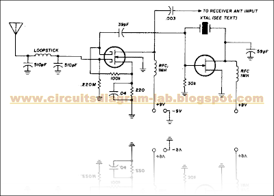
This is The Simple Vlf Converter Circuit Diagram. This converter uses a low-pass filter instead of the usual tuned circuit so the only tuning required is with the receiver. The dual-gate MOSFET and FET used in the mixer and oscillator aren`t critical. 

Simple Vlf Converter Circuit Diagram


Simple Vlf Converter Circuit Diagram
 
Any crystal having a frequency compatible with the receiver tuning range may be used. For example, with a 3500 kHz crystal, 3500 kHz on the receiver dial corresponds to zero kHz; 3600 to 100 kHz; 3700 to 200 kHz, etc (At 3500 khz on the receiver all one can hear is the converter oscillator, and VLF signals start to come in about 20 kHz higher).
Continue reading...

Simple F and V Converter Circuit Diagram

This is a best Frequency/Voltage Converter circuit diagram proportional voltage by the use of a frequency-to-voltage (F/V) converter. Teledyne Semiconductor`s Type TSC9402 is a versatile IC. Not only can it convert voltage into frequency, but also frequency into voltage. It is thus eminently suitable for use in an add-on unit for measuring frequencies with a multimeter. 

 Best F and V Converter Circuit Diagram


Best F and V Converter Circuit Diagram


Only a few additional components are required for this.. Just one calibration point sets the center of the measuring range (or of that part of the range that is used most frequently). The frequency-proportional direct voltage at the output (pin 12—amp out) contains interference pulses at levels up to 0.7 V. If these have an adverse effect on the multimeter, they can be suppressed with the aid of a simple RC network. 

The output voltage, U0, is calculated by: tfo=C/rei(Ci + 12 pF) R2fm Because the internal capacitance often has a greater value than the 12 pF taken here, the formula does not yield an absolute value. The circuit has a frequency range of dc to 10 kHz. At 10 kHz, the formula gives a value of 3.4 V. The circuit draws a current of not more than 1 mA. 

Sourced By : Circuitsstream
Continue reading...

Simple Solar Relay Circuit Diagram

Build a Simple Solar Relay Circuit Diagram.With extended periods of bright sunshine and warm weather, even relatively large storage batteries in solar-power systems can become rather warm. Consequently, a circuit is usually connected in parallel with the storage battery to either connect a high-power shunt (in order to dissipate the excess solar power in the form of heat) or switch on a ventilation fan via a power FET, whenever the voltage rises above approximately 14.4 V. However, the latter option tends to oscillate, since switching on a powerful 12-V fan motor causes the voltage to drop below 14.4 V, causing the fan to be switched off. In the absence of an external load, the battery voltage recovers quickly, the terminal voltage rises above 14.4 V again and the switching process starts once again, despite the built-in hysteresis.

 Simple Solar Relay Circuit Diagram

Simple Solar Relay Circuit Diagram

A solution to this problem is provided by the circuit shown here, which switches on the fan in response to the sweltering heat produced by the solar irradiation instead of an excessively high voltage at the battery terminals. Based on experience, the risk of battery overheating is only present in the summer between 2 and 6 pm. The intensity of the sunlight falling within the viewing angle of a suitably configured ‘sun probe’ is especially high precisely during this interval. This is the operating principle of the solar relay.
The trick to this apparently rather simple circuit consists of using a suitable combination of components. Instead of a power FET, it employs a special 12-V relay that can handle a large load in spite of its small size. This relay must have a coil resistance of at least 600 Ω, rather than the usual value of 100-200 Ω. This requirement can be met by several Schrack Components relays (available from, among others, Conrad Electronics). Here we have used the least expensive model, a type RYII 8-A printed circuit board relay. The light probe is connected in series with the relay. It consists of two BPW40 photo-transistors wired in parallel.
The type number refers to the 40-degree acceptance angle for incident light. In bright sunlight, the combined current generated by the two photo-transistors is sufficient to cause the relay to engage, in this case without twitching. Every relay has a large hysteresis, so the fan connected via the a/b contacts will run for many minutes, or even until the probe no longer receives sufficient light. The NTC thermistor connected in series performs two functions. First, it compensates for changes in the resistance of the copper wire in the coil, which increases by approximately 4 percent for every 10 ºC increase in temperature, and second, it causes the relay to drop out earlier than it otherwise would (the relay only drops out at a coil voltage of 4 V).

Depending on the intended use, the 220-Ω resistance of the thermistor can be modified by connecting a 100-Ω resistor in series or a 470-Ω resistor in parallel. If the photo-transistors are fastened with the axes of their incident-angle cones in parallel, the 40-degree incident angle corresponds to 2 pm with suitable solar orientation. If they are bent at a slight angle to each other, their incident angles overlap to cover a wider angle, such as 70 degrees. With the tested prototype circuit, the axes were oriented nearly parallel, and this fully met our demands. The automatic switch-off occurs quite abruptly, just like the switch-on, with no contact jitter. This behavior is also promoted by the NTC thermistor, since its temperature coefficient is opposite to that of the ‘PTC’ relay coil and approximately five times as large.
This yields exactly the desired effect for energizing and DE-energising the relay: a large relay current for engagement and a small relay current for disengagement. Building the circuit is actually straightforward, but you must pay attention to one thing. The photo transistors resemble color less LEDs, so there is a tendency to think that their ‘pinning’ is the same as that of LEDs, with the long lead being positive and the short lead negative. However, with the BPW40 the situation is exactly the opposite; the short lead is the collector lead. Naturally, the back-emf diode for the relay must also be connected with the right polarity. The residual current on cloudy days and at night is negligibly small. 
Continue reading...

Simple Miser Flash Circuit Diagram

A flashing LED at the doorstep of your garage or home will trick the thieves into believing that a sophisticated security gadget is installed. The circuit is nothing but a low-current drain flasher. It uses a single CMOS timer that is configured as a free running oscillator using a few additional components. As the LED flashes very briefly, the average current through the LED is around 150 µA with a high peak value, which is sufficient for normal viewing. This makes it a real miser.

The 9V battery source is connected via ‘on’/‘off’ switch S1 to the circuit. When switch S1 is closed, the IC receives power from capacitor C1, which is constantly charged through resistor R1. As capacitor C1 delivers power to IC1, it saves the battery from drain.

 Simple Miser Flash Circuit Diagram
 

Most LEDs consume a current of 20 mA, which in many instances is higher than the power consumed by the rest of the circuit. This is undesirable if the device is battery-powered. In this circuit, the energy consumed by the LED is a small fraction of the normal value. Capacitor C2 charges through resistor R2 and diode D1. 

When the voltage across C2 reaches two-third of the supply voltage, threshold pin 7 of IC1 switches on as a current sink. The capacitor discharges through LED1 into pin 7 rapidly. Diode 1N4148 (D1) provides the one-way charging path for capacitor C2 via resistor R2. LED1 illuminates briefly for a while with the accumulated charges in C2. Again, the charging cycle repeats. This way, LED continues flashing. A 9V PP3 battery can perfectly handle this job.


Sourced by: EFY. Author  T.A. Babu
Continue reading...

Simple Burglar Alarm Circuit Diagram

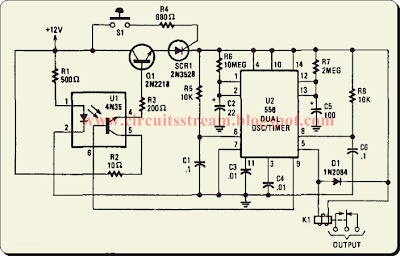
This is the simple burglar alarm with timed shutoff. In this circuit when SI (sensor) is closed, power is applied to U2, a dual timer. After a time determined by C2, CI is energized after a predetermined time determined by the value of C5, pin 9 of U2 becomes low, switching off the transistor in the opt isolator, cutting anode current of SCR1 and de-energizing Kl. The system is now reset. 

 Simple Burglar Alarm Circuit Diagram


Simple Burglar Alarm Circuit Diagram


Notice that (i6x C2) is less than (R7xC$). The ON time is approximately given by:(R7xC5)-(R6xC2) = Ton 
Continue reading...

Sunday, December 22, 2013

Ultra Simple Microphone Preamplifier

This little project came about as a result of a design job for a client. One of the items needed was a mic preamp, and the project didnt warrant a design such as the P66 preamp, since it is intended for basic PA only. Since mic preamps are needed by people for all manner of projects, this little board may be just whats needed for interfacing a balanced microphone with PC sound cards or other gear. Unlike most of my boards, this one is double-sided. I normally avoid double-sided PCBs for projects because rework by those inexperienced in working with them will almost certainly damage the board beyond repair.

I consider this not to be an issue with this preamp, because it is so simple. It is extremely difficult to make a mistake because of the simplicity. As you can see, the board uses a PCB mounted XLR connector and pot, so is a complete mic preamp, ready to go. Feel free to ignore the terminals marked SW1 (centred between the two electrolytic supply caps), as they are specific to my clients needs and are not useful for most applications. The original use was to use them for a push-button switch that activated an audio switch via a PIC micro-controller. They are not shown on the schematic.

Ultra-Simple Microphone Preamplifier Image Project :
 P12-pic
The DC, GND and output terminals may be hard wired to the board, you may use PCB pins or a 10-way IDC (Insulation Displacement Connector) and ribbon cable. Power can be anything between +/-9V and +/-18V with an NE5532 opamp. The mic input is electronically balanced, and noise is quite low if you use the suggested opamp. Gain range is from about 12dB to 37dB as shown. It can be increased by reducing the value of R6, but this should not be necessary. Because anti-log pots are not available, the gain control is not especially linear, but unfortunately in this respect there is almost no alternative and the same problem occurs with all mic preamps using a similar variable gain control system.

Ultra-Simple Microphone Preamplifier Circuit diagram:

P12-f1

The circuit is quite conventional, and if 1% metal film resistors are used throughout it will have at least 40dB of common mode rejection with worst-case values. The input capacitors give a low frequency rolloff of -3dB at about 104Hz. If better low frequency response is required, these caps may be increased to 4.7uF or 10uF bipolar electrolytics. These will give response to well below 10Hz if you think youll ever need to go that low. The project PCB measures 77 x 24mm, and the mounting centers for the pot and XLR connector are spaced at 57mm. If preferred, a traditional chassis mounted female XLR can be used, and wired to the board with heavy tinned copper wire. The PCB pads for the connector are in the correct order for a female chassis mount socket mounted with the "Push" tab at the top.

source:  http://www.ecircuitslab.com/2011/08/ultra-simple-microphone-preamplifier.html
Continue reading...

Saturday, December 21, 2013

Simple Switching Regulator Circuit Diagram

This is the simple switching regulator circuit diagram. The LTC10432 switched-capacitor building block provides nonoverlapping complementary drive to the Ql to Q4 power MOSFETs. The MOSFETs are arranged so that Cl and C2 are alternately placed in series and then parallel. During the series phase, the + 12 V battery`s current flows through both capacitors, charging them, and furnishing load current. 

During the parallel phase, both capacitors deliver current to the load. Ql and Q2 receive similar drive from pins 3 and 11. The diode-resistor networks provide additional nonoverlapping drive characteristics, preventing simultaneous drive to the series-parallel phase switches. Normally, the output would be one-half of the supply voltage, but C1 and its associated components close a feedback loop, forcing the output to 5 V. With the circuit in the series phase, the output heads rapidly positive. 

When the output exceeds 5 V, Cl trips, forcing the LTC1043 oscillator pin, trace D, high; this truncates the LTC1043`s triangular-wave oscillator cycle. The circuit is forced into the parallel phase and the output coasts down slowly, until the next LTC1043 clock cycle begins. Cl`s output diode prevents the triangle down-slope from being affected and the 100-pF capacitor provides sharp transitions. The loop regulates the output to 5 V by feedback controlling the turn-off point of the series phase.

Simple Switching Regulator Circuit Diagram


Continue reading...

Simple 0 50V 2A Bench Power Supply Circuit Diagram

I use the lm10 IC because it has a reference voltage and that’s useful for dc power supply. With two ICs can take different output voltage and amperage. This circuit is protected from short circuit.P2 is for controlling the current at the range of 0-2A. Stabilize the output voltage with R4 on negative pin on op-amp and with R2 & P1 on positive pin. 

0-50V 2A Bench Power Supply Circuit Diagram

Simple 0-50V 2A Bench Power Supply Circuit Diagram
 
 Op-amp output controls T1 that not let ripple of voltage.T1 increase or decrease ampere of R6 and control the voltage of T5 & T4. Pin 1 is the reference voltage and reference voltage is losing some voltage on R1 that has 100uA . This current passes through P1 too.
Vlose p1=100uA*Rp1

This lose voltage regulate output voltage rate of output current is compare between reference voltage of P3 and lose voltage on R11.T3 is protecting short circuit with R11. For reduce out put voltage to 0v should parallel one resistor 470 ohm in out put. Minimum voltage is 0.4v. The maximum output voltage is fixed with R1b and should not become over of 50v. Therefore your transformer should give 36V, 3A with 4700uF capacitor. T6, T5, T7 need heatsilk.

Simple 0-50V 2A Bench Power Supply Circuit Diagram pcb


R1a = 2,2 K
R1b = read the text
R2 = 10 K
R3, R7 = 3.3 k
R4 = 390 Ohm
R5 = 47 K
R6 = 3.3 K 1Watt
R8 = 180 Ohm
R9, R10 = 0.47 Ohm 3Watt
R11 = 0.075 Ohm 2Watt
R12 = 470 Ohm
P1 = 500K liner potentiometer
P2 = 4.7 K potentiometer
P3 = 10 K potentiometer
C1 = 1nF
C2 = 10nF
C3 = 22nF
C4 = 47mF 63v electrolytic
C5 = 4700mF 80v electrolytic
T1, T2 = BC161
T3, T4 = BD141
T5 = BD241
T6, T7 = 2V3055
D1, D2 = 1N4148
D3, D4 = 1N4001
IC1, IC2 = LM10C
Continue reading...

Thursday, December 19, 2013

Simple FM Transmitter Circuit Schematic

This is a simplest FM transmitter circuit schematic with a single transistor. It build with a very few numbers of components include a transistor, few capacitors, resistors and a small microphone.

Circuit Diagram 

simple-fm-transmitter

Circuit Description

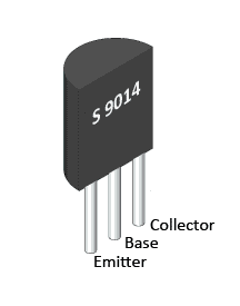
A S9014 NPN transistor is used here; you can use BC547 as an alternative of it. All the capacitor used in circuit is ceramic capacitor. Don’t be surprised with the supply voltage of 1.5 volt. Here you can use a single 1.5V AA battery cell, or a 3V battery that will be endurable for this this FM transmitter circuit. A small microphone used here is an electret condenser type microphone (see below). Must use at least a small antenna for a higher transmitting-range. Then try with a bigger antenna for increasing range. 

Transistor S9014 Pinout

S9014 Pinout

Electret condenser type microphone

Electret condenser microphone


If you have any confusion about capacitor value, check this.
Continue reading...

Thursday, October 3, 2013

Simple Cat 5 Network Tester

This circuit came from a need for a "quick and dirty" network tester that could be operated by one person. All the commercial units I tried required a person at the other end to check the remote LEDs, as the transmitters could not be made to cycle through the test continuously to allow one person to check both ends. It must be noted that this unit will only check for pair continuity, pair shorts, crossed wires, and shorts to other pairs. It will not test bandwidth, etc. Operation is fairly basic.


Half of the 4011 quad 2-input NAND gate is an RS flip-flop (IC1a, IC1b) which controls the other half, IC1c & IC1d, operating as a clock oscillator. You can either start and stop the oscillator running by pressing the Start and Stop switches or by virtue of diode D1 connected to pins 12 & 13, use the Stop switch to allow manual clocking of the 4017 counter. The 4017 drives one of eight LEDs and the lines to the RJ45 socket. An output "High" on the 4017 decides which line is under test, and if the circuit is complete, the test LEDs current is "sunk" by the 4017 and the LED will light.

If the corresponding test LED on the remote fails to light, then there is a short of that pair in the cable under test. If more than one LED lights, it indicates a short with another pair. A dark test LED on the transmitter indicates that pair is open circuit. "Start" starts the circuit cycling at a rate determined by the 470nF capacitor and 220kO resistor and "Stop/Step" stops cycling, steps through the lines, and when stepped so that no channel LEDs are alight, effectively switches the unit off with a standby drain current of less than a microamp.
Continue reading...

Thursday, September 26, 2013

Simple BFO Metal Locator

This circuit uses a single coil and nine components to make a particularly sensitive low-cost metal locator. It works on the principle of a beat frequency oscillator (BFO). The circuit incorporates two oscillators, both operating at about 40kHz. The first, IC1a, is a standard CMOS oscillator with its frequency adjustable via VR1. The frequency of the second, IC1b, is highly dependent on the inductance of coil L1, so that its frequency shifts in the presence of metal. L1 is 70 turns of 0.315mm enamelled copper wire wound on a 120mm diameter former. The Faraday shield is made of aluminium foil, which is wound around all but about 10mm of the coil and connected to pin 4 of IC1b.

Simple BFO metal locator circuit schematic

The two oscillator signals are mixed through IC1c, to create a beat note. IC1d and IC1c drive the piezo sounder in push-pull fashion, thereby boosting the output. Unlike many other metal locators of its kind, this locator is particularly easy to tune. Around the midpoint setting of VR1, there will be a loud beat frequency with a null point in the middle. The locator needs to be tuned to a low frequency beat note to one or the other side of this null point. Depending on which side is chosen, it will be sensitive to either ferrous or non-ferrous metals. Besides detecting objects under the ground, the circuit could serve well as a pipe locator.
Continue reading...

Wednesday, September 11, 2013

Simple Hard Disk Selector Circuit Diagram

Hard Disk Selector Circuit Diagram
 
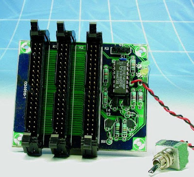
In the last few years, the available range of operating systems for PCs  has increased dramatically. Various free (!) operating systems have been  added to the list, such as BeOS, OpenBSD and Linux. These systems are  also available in different colours and flavours (versions and  distributions). Windows is also no longer simply Windows, because there  are now several different versions (Windows 95, 98, ME, NT, XP, Vista  and 7). Computer users thus have a large variety of options with regard  to the operating system to be used. One problem is that not all hardware  works equally well under the various operating systems, and with regard  to software, compatibility is far from being universal. In other words,  it’s difficult to make a good choice.

Hard Disk Selector Circuit Diagram

Hard Disk Selector Circuit Diagram


Switching from one operating system to another - that’s a risky business, isn’t it? Although this may be a bit of an exaggeration, the safest approach is still to install two different operating systems on the same PC, so you can always easily use the ‘old’ operating system if the new one fails to meet your needs (or suit your taste). A software solution is often used for such a ‘dual system’. A program called a ‘boot manager’ can be used to allow the user to choose, during the start-up process, which hard disk will be used for starting up the computer. Unfortunately, this does not always work flawlessly, and in most cases this boot manager is replaced by the standard boot loader of the operating system when a new operating system is installed.

In many cases, the only remedy is to reinstall the software. The solution presented here does not suffer from this problem. It is a hardware solution that causes the primary and secondary hard disk drives to ‘swap places’ when the computer is started up, if so desired. From the perspective of the computer (and the software running on the computer), it appears as though these two hard disks have actually changed places. This trick is made possible by a feature of the IDE specification called ‘CableSelect’. Every IDE hard disk can be configured to use either Master/Slave or CableSelect. In the latter case, a signal on the IDE cable tells the hard disk whether it is to act as the master or slave device. For this reason, in every IDE cable one lead is interrupted between the connectors for the two disk drives, or the relevant pin is omitted from the connector.

pcb

pcb

This  causes a low level to be present on the CS pin of one of the drives and  a high level to be present on the CS pin of the other one (at the far  end of the cable). The circuit shown here is connected to the IDE bus of  the motherboard via connector K1. Most of the signals are fed directly  from K1 to the other connectors (K2 and K3). An IDE hard disk is  connected to K2, and a second one is connected to K3. When the computer  is switched on or reset, a pulse will appear on the RESET line of the  IDE interface. This pulse clocks flip-flop IC1a, and depending on the  state of switch S1, the Q output will go either high or low. The state  on the Q output is naturally always the opposite of that on the Q  output. If we assume that the switch is closed during start-up, a low  level will be present on D input of IC1a, so the Q output will be low  following the reset pulse.


Continue reading...

Tuesday, September 3, 2013

Simple 4 Channel Video Amplifier Using NJM2582

A very simple 4 channel video amplifier electronic circuit project can be designed using NJM2582 ic suitable for video applications with SCART connector . Design of the circuit is very simple and require few external electronic parts .

Simple 4 Channel Video Amplifier Circuit diagram


Some features of the NJM2582 are : Operating Voltage ±5V, +5V, +11V ; 6input 4output , 2input 1output Video SW , Internal LPF , 6dB Amplifier , Internal 75Ω Driver Circuit , DC output for SCART (FUNCTION SW, BLANKING) .
Continue reading...

Monday, September 2, 2013

Simple Light Alarm Schematic

A very simple light alarm schematic circuit project can be designed using some common electronic parts, as you can see in the circuit diagram bellow . This light alarm schematic circuit project will sound as soon as the drawer is opened and light falls on the Darlington phototransistor. The output alarm may be redesigned to activate a relay or triac. This simple light alarm schematic circuit project use a MAL12 LDR photoresistor as a sensor .

Light Alarm Schematic Circuit diagram


The 14011 quad , 2 input, NAND gate is wired up to oscillate when the input to it goes high, that is the BC557 transistor turns on after light is detected by the MAL12. The oscillating output from the 14011 turns the BC547 on and off , making the buzzer to sound. After the alarm has started and it is put back into dark conditions , alarm will continue to sound for about 3 - 5 seconds. This is due to the 1uF capacitor and 4M7 resistor which keep the input to the 14011 high .

The circuit is very simple and must be powered from a simple 9 volts DC power supply or a 9 volt battery .
Continue reading...

Saturday, August 31, 2013

Simple Circuit Transistor Checker

This simple circuit has helped me out on many occasions. It is able to check transistors, in the circuit, down to 40 ohms across the collector-base or base-emitter junctions. It can also check the output power transistors on amplifier circuits.

Simple Circuit Transistor Checker Schematic

Circuit operation is as follows. The 555 timer ( IC1 ) is set up as a 12hz multi vibrator. The output on pin 3 drives the 4027 flip-flop ( IC2). This flip-flop divides the input frequency by two and delivers complementary voltage outputs to pin 15 and 14. The outputs are connected to LED1 and LED2 through the current limiting resistor R3. The LEDs are arranged so that when the polarity across the circuit is one way only one LED will light and when the polarity reverses the other LED will light, therefore when no transistor is connected to the tester the LEDs will alternately flash.

The IC2 outputs are also connected to resistors R4 and R5 with the junction of these two resistors connected to the base of the transistor being tested. With a good transistor connected to the tester, the transistor will turn on and produce a short across the LED pair. If a good NPN transistor is connected then LED1 will flash by itself and if a good PNP transistor is connected then LED2 will flash by itself. If the transistor is open both LEDs will flash and if the transistor is shorted then neither LED will flash.
Continue reading...