Sunday, November 2, 2014
AUTOMATIC AIRFLOW DETECTOR ELECTRONIC DIAGRAM
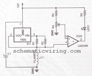
Sensor used in this circuit is a bulb filament. If there is no airflow, the filament resistance would give low value. On the other hand, if there is airflow, the filament resistance would varies. The variation of the resistance is caused by the heat difference between filament. It also effects to the voltage variation passing through that filament. That voltage difference will be processed by LM339 op-amp and displayed by the LED.
Parts list :
- LED1 : LED 5mm
- IC1 volt regulator : LM7805
- Polar Capacitor C1 : 47 uF/15V
- Resistor R1 : 100 ohm
- Resistor R2 : 470 ohm
- Resistor R3 : 10k ohm
- Potensiometer R4 : 100k ohm
- Resistor R5 : 1k ohm
- IC2 op-amp : LM339
- Bulb filament
- Power supply/battery 12V

Wednesday, October 29, 2014
Electronic Motor Starter Diagram Circuit
 Switch S1 is used to turn on the pump, while switch S2 is used to turn off the pump. While making over-/under-voltage setting, disconnect C2 temporarily. Capacitor C2 prevents relay chattering due to rapid voltage fluctuations. Regulator IC 7809 gives the 9V regulated supply to soft switch as well as the relay after filtering by capacitor C4. A suitable miniature circuit breaker is used for automatic over-current protection. Green LED (LED1) indicates that the motor is ‘on’ and red LED (LED2) indicates that the power is ‘on’. The motor is connected to the normally-open contact of the relay. When the relay energizes, the motor turns on.
Tuesday, October 28, 2014
LM3909 IC bassed Color organ electronic project
Using LM 3909 LED flasher IC , can be designed various electronic projects . As you can see in this circuit diagram , using the LM3909 LED flasher IC can be designed a very simple color organ .
This circuit is not complicated , it use just some common active audio filters for filtering audio signals and a part formed by a LM3909 IC .
All of three active filters drives the audio spectrum into three bands drive rectifiers and then drive IC2,3 and 4 , flashing the LEDs at 6 Hz. D4,D5 and D6 should be three different colors for best effect .
In the table bellow you can see all electronic parts required by this color organ project .
Friday, October 4, 2013
Electronic Die
The electronic die also uses energy efficiently by driving the display in pulsed mode. As a result of the latter two features, the current consumption of the circuit is approximately 25 mA in use and 12 mA in standby. This means that it can easily be powered by a 9-V battery. The circuit consists of the following parts: a free-running oscillator (IC1a), additional logic for driving the display (IC1c & IC1d), a timer (IC1b), a counter (IC3) and a display decoder (IC2). The oscillator is very simple. Its frequency, which is determined by R1 and C1, is approximately 225 Hz, with a duty cycle of around 50–60 percent. The signal from the oscillator acts as a clock signal for the counter (via R2) and a blanking signal for the display decoder (via IC1d).
 However, the counter will not count as long as the ‘throw’ switch (S1) remains closed, since the clock input of IC3 is grounded by S1. The blanking input of the display decoder is driven by a pulse waveform, so the display is in principle illuminated only around 50 percent of the time, but it appears to be constantly illuminated due to the high clock frequency. The standby mode works as follows. As long as there is a signal on the clock input of the counter (S1 pressed), the output of gate IC1b is low and the display is enabled. If S1 is released, the counter stops and a number will be shown on the display. However, the clock pulses will have charged C2 via D1, and C2 will slowly discharge via R4.
After approximately 8 seconds, the output of gate IC1b will go high, causing the display to be blanked. The design of the counter is relatively simple. It is wired as an up counter by connecting the U/D pin to VCC. The preset inputs (pins 4, 12, 13 and 3) are configured to binary ‘0001’, and the counter normally has a counting range of 0–9 (pin 9 connected to ground). Diodes D2, D3 and D4, in combination with resistor R5, act as a logic AND gate, so if the value of the counter is greater than 6, the preset value of 1 is latched into the counter and it starts to count again from 1 to 6. This only happens if jumper J1 is open. If it is closed, the preset pulse on PREN is suppressed and the counter range is 0–9. The A, B, C and D inputs of the decoder IC (IC2) are driven directly by the counter.
The series resistors normally used for the individual segments of the display are instead placed in the common-cathode lead (R7 & R8). This has the advantage of allowing the number of resistors to be reduced, although it has the drawback that the brightness of the display depends on the displayed number. If the segment current is sufficiently large, (light) saturation occurs and this brightness variation is no longer noticeable. The Blank input (BL) controls whether the display is enabled. If you choose to build this circuit using SMD technology, that will not affect the schematic diagram, but it will naturally affect the choice of components. In this case, SMD components must be used for the resistors and C1, the diodes must be replaced by BAS32 types, and BT versions of ICs IC1–IC3 must be used instead of conventional types.
An SMD version of C2 was not used in the prototype, since SMD electrolytic capacitors are expensive, and normally they are only sold in lots of 10, just like other passive components. It is also recommended to use a socket for the display of the SMD version of the electronic die, to allow the space under the display to also be used and the dimensions of the circuit board to be further reduced. Any desired DC power source providing a voltage of 5 to 15 V can be used as a power supply. Due to the low current consumption of the circuit, a 9-V battery will last quite a long time.
Wednesday, October 2, 2013
Electronic Cricket Match Game
Output from IC1 passes into the input of IC2 which is the popular Johnson Decade counter CD4017. It has 10 outputs. Of these 8 outputs are used. Output 9 ( pin9) is tied to the reset pin 15 to repeat the cycle. When the input pin 14 of IC2 gets low to high pluses, its output turns high one by one. Resistor R3 keeps the input of IC2 low in stand by state to avoid false indications.
Electronic Cricket Circuit Diagram

Tuesday, October 1, 2013
Electronic Telephone Ringer Circuit
This circuit produces a ringing sound similar to that made by more recent telephones. It consists of three almost identical oscillators connected in a chain, each generating a squarewave signal. The frequency of each oscillator depends on the RC combination: R4 and C1 around IC1.A, R8 and C2 around IC1.B and R12 and C3 around IC3.C. The pairs of 100 kΩ resistors divide the asymmetric power supply voltage (between 5 V and 30 V) so that, in conjunction with the 100 kΩ feedback resistors (R3, R7 and R11) either one third or two thirds of the supply voltage will be present at the non-inverting inputs to the opamps. The voltage across the capacitor therefore oscillates in a triangle wave between these two values.
Circuit Diagram :
 Electronic Telephone Ringer Circuit Diagram
The first oscillator is free-running at a frequency of approximately 1/3 Hz. Only when its output is high, and D1 stops conducting, can the second oscillator run. The frequency of the second oscillator is about 13 Hz, and optional LED D3 flashes when it is running. When the output of the second oscillator is low, the third is allowed to run. The frequency of the third oscillator is around 1 kHz, and this is the tone that is produced. The second oscillator is not absolutely necessary: its function is just to add a little modulation to the 1 kHz tone. A piezo sounder is connected to the output of the third oscillator to convert the electrical signal into an acoustic one. The current consumption of the circuit is just under 1mA with a 5V power supply, rising to about 1.65mA with a supply voltage of 15 V.
Author: L. Libertin Copyright: Elektor Electronics
Electronic Die
The simplicity of a traditional die makes it exceptionally difficult to create a fully equivalent electronic version, if only because an electronic version requires a power supply and a collection of electronic components that occupy a much larger volume than a normal die. This article describes an electronic die that can be built using normal components or SMDs as desired, and which comes very close to having the same format as a traditional die in the latter case. Despite its simplicity, this electronic die incorporates several interesting features. For instance, the range of ‘spots’ can be increased from 1–6 to 0–9 using a jumper, and it has standby function that disables the display approximately 8 seconds after the die has been ‘thrown’, in order to save energy.
The electronic die also uses energy efficiently by driving the display in pulsed mode. As a result of the latter two features, the current consumption of the circuit is approximately 25 mA in use and 12 mA in standby. This means that it can easily be powered by a 9-V battery. The circuit consists of the following parts: a free-running oscillator (IC1a), additional logic for driving the display (IC1c & IC1d), a timer (IC1b), a counter (IC3) and a display decoder (IC2). The oscillator is very simple. Its frequency, which is determined by R1 and C1, is approximately 225 Hz, with a duty cycle of around 50–60 percent. The signal from the oscillator acts as a clock signal for the counter (via R2) and a blanking signal for the display decoder (via IC1d).

However, the counter will not count as long as the ‘throw’ switch (S1) remains closed, since the clock input of IC3 is grounded by S1. The blanking input of the display decoder is driven by a pulse waveform, so the display is in principle illuminated only around 50 percent of the time, but it appears to be constantly illuminated due to the high clock frequency. The standby mode works as follows. As long as there is a signal on the clock input of the counter (S1 pressed), the output of gate IC1b is low and the display is enabled. If S1 is released, the counter stops and a number will be shown on the display. However, the clock pulses will have charged C2 via D1, and C2 will slowly discharge via R4.
After approximately 8 seconds, the output of gate IC1b will go high, causing the display to be blanked. The design of the counter is relatively simple. It is wired as an up counter by connecting the U/D pin to VCC. The preset inputs (pins 4, 12, 13 and 3) are configured to binary ‘0001’, and the counter normally has a counting range of 0–9 (pin 9 connected to ground). Diodes D2, D3 and D4, in combination with resistor R5, act as a logic AND gate, so if the value of the counter is greater than 6, the preset value of 1 is latched into the counter and it starts to count again from 1 to 6. This only happens if jumper J1 is open. If it is closed, the preset pulse on PREN is suppressed and the counter range is 0–9. The A, B, C and D inputs of the decoder IC (IC2) are driven directly by the counter.
The series resistors normally used for the individual segments of the display are instead placed in the common-cathode lead (R7 & R8). This has the advantage of allowing the number of resistors to be reduced, although it has the drawback that the brightness of the display depends on the displayed number. If the segment current is sufficiently large, (light) saturation occurs and this brightness variation is no longer noticeable. The Blank input (BL) controls whether the display is enabled. If you choose to build this circuit using SMD technology, that will not affect the schematic diagram, but it will naturally affect the choice of components. In this case, SMD components must be used for the resistors and C1, the diodes must be replaced by BAS32 types, and BT versions of ICs IC1–IC3 must be used instead of conventional types.
An SMD version of C2 was not used in the prototype, since SMD electrolytic capacitors are expensive, and normally they are only sold in lots of 10, just like other passive components. It is also recommended to use a socket for the display of the SMD version of the electronic die, to allow the space under the display to also be used and the dimensions of the circuit board to be further reduced. Any desired DC power source providing a voltage of 5 to 15 V can be used as a power supply. Due to the low current consumption of the circuit, a 9-V battery will last quite a long time.
Source : www.extremecircuits.net
Tuesday, September 10, 2013
Electronic Security Door Key Circuit Diagram

Part List
R1-7-9=1Kohm
R2-3-4-5=100Kohm
R6 =10Kohm
R9 =47Kohm
IC1 = 4066
IC2 =4N25
Q1-2=BC550
S1...11=Push button sw or keyboard
S12=Push button normal closed
All resistors is 1/4W 5%
Tuesday, September 3, 2013
Schematic 10 Way Electronic Switch
10 Way Electronic Switch Circuit Diagram

The schematic is shown above, and two switches S1 and S2 are used to control the outputs. The main work is done by U2 a CMOS4017 decade counter divider IC. At switch on, C1 is quickly charged by R4 and a brief reset pulse is applied to to the reset pins of both U1 and U2. This results in U1, a 7 segment display display driver and decade counter showing "zero" on the 7 segment display and pin 3 (which is the output zero) of the 4017 becoming high.
Each time S1 is pressed the clock input of U2 is incremented, by one count and the display and 4017 will cycle through all 10 outputs. A separate reset switch is not provided as the display reads the currently selected output.
When the 4017 is on a particular output, for example zero, then the controlled circuit can be turned on or off using switch S2. To latch the output a type JK flip-flop is used at each of the ten outputs. This works as follows. When the 4017 is at output zero, pin 3 will be high. This enables both JK inputs of the flip flop (U4A at output zero) and the circuit can then be toggled via pulses applied from switch S2. The Q output of each flip-flop drives and NPN transistor and then a small relay. The NPN transistors can be any general purpose type, e.g. 2N2222, BC108, BC548 etc. The relay allows external loads of different voltage and current to this circuit to be controlled.
For clarity, the schematic is drawn with outputs, zero, six and nine shown only. The pinouts for the CMOS ICs 4017 and 4026 can be found in the practical section.
The CMOS 4026 is available at ESR Electronics in the UK.
If required, the external circuits power supply can be used to power the driver transistor and relay. This is shown on output 6, the dotted lines representing the power coming from an external battery. The only other requirement here is that the external circuits common negative terminal is tied to this circuits common chassis (negative) terminal.
Saturday, December 1, 2012
Peak Electronic Design Limitedethernet Wiring Diagramspatch

Peak Electronic Design Limited Ethernet Wiring Diagrams Patch.

Cat5e Wiring.

Gefen Component Audio Over Cat5 Wiring Diagram.

Terminating Rj 45 Cat5 Cat5e Cat6 Data.

An Ethernet And Phone Jack Using A Single Cat5e Cable Mavromatic.

Wiring Diagram For An Ethernet Crossover Cable.

Cat 5 Wiring Diagram Crossover Cable Diagram.

Structured Wiring Retro Install 1.

Cat 5 Wiring Diagram Crossover Cable Diagram.

Rj45 Pinout Wiring How To Make Up A 10baset 100baset Connection Eia.